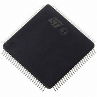
ST10F276Z5T3 STMicroelectronics, ST10F276Z5T3 Datasheet - Page 134

ST10F276Z5T3
Manufacturer Part Number
ST10F276Z5T3
Description
MCU 16BIT 832KBIT FLASH 144-TQFP
Manufacturer
STMicroelectronics
Series
ST10r
Datasheet
1.ST10F276Z5T3.pdf
(239 pages)
Specifications of ST10F276Z5T3
Core Processor
ST10
Core Size
16-Bit
Speed
40MHz
Connectivity
ASC, CAN, EBI/EMI, I²C, SSC, UART/USART
Peripherals
POR, PWM, WDT
Number Of I /o
111
Program Memory Size
832KB (832K x 8)
Program Memory Type
FLASH
Ram Size
68K x 8
Voltage - Supply (vcc/vdd)
4.5 V ~ 5.5 V
Data Converters
A/D 24x10b
Oscillator Type
Internal
Operating Temperature
-40°C ~ 125°C
Package / Case
144-TQFP, 144-VQFP
Cpu Family
ST10
Device Core Size
16b
Frequency (max)
40MHz
Interface Type
CAN/I2C
Total Internal Ram Size
68KB
# I/os (max)
111
Number Of Timers - General Purpose
5
Operating Supply Voltage (typ)
5V
Operating Supply Voltage (max)
5.5V
Operating Supply Voltage (min)
4.5V
On-chip Adc
24-chx10-bit
Instruction Set Architecture
CISC/RISC
Operating Temp Range
-40C to 125C
Operating Temperature Classification
Automotive
Mounting
Surface Mount
Pin Count
144
Package Type
LQFP
Processor Series
ST10F27x
Core
ST10
Data Bus Width
16 bit
Data Ram Size
68 KB
Maximum Clock Frequency
40 MHz
Number Of Programmable I/os
111
Number Of Timers
5
Maximum Operating Temperature
+ 125 C
Mounting Style
SMD/SMT
Minimum Operating Temperature
- 40 C
For Use With
497-6399 - KIT DEV STARTER ST10F276Z5
Lead Free Status / RoHS Status
Lead free / RoHS Compliant
Eeprom Size
-
Lead Free Status / Rohs Status
Compliant
Available stocks
Company
Part Number
Manufacturer
Quantity
Price
Company:
Part Number:
ST10F276Z5T3
Manufacturer:
STMicroelectronics
Quantity:
10 000
Power reduction modes
20.3.1
134/239
In normal running mode (that is when main V
during reset to exercise the EA functionality associated with the same pin: the voltage
supply for the circuitries which are usually biased with V
oscillator used in conjunction with real-time clock module), is granted by the active main
V
It must be noted that Standby mode can generate problems associated with the usage of
different power supplies in CMOS systems; particular attention must be paid when the
device I/O lines are interfaced with other external CMOS integrated circuits: if V
becomes (for example in Standby mode) lower than the output level forced by the I/O lines
of these external integrated circuits, the device could be directly powered through the
inherent diode existing on device output driver circuitry. The same is valid for the device
interfaced to active/inactive communication buses during Standby mode: current injection
can be generated through the inherent diode.
Furthermore, the sequence of turning on/off of the different voltage could be critical for the
system (not only for the device). The device Standby mode current (I
V
V
phenomenon.
Entering Standby mode
As already said, to enter Standby mode XRAM2EN bit in the XPERCON Register must be
cleared: this allows to freeze immediately the RAM interface, avoiding any data corruption.
As a consequence of a RESET event, the RAM Power Supply is switched to the internal
low-voltage supply V
The RAM interface will remain frozen until the bit XRAM2EN is set again by software
initialization routine (at next exit from main V
Since V
XRAM2EN bit is no longer able to guarantee its content (logic “0”), being the XPERCON
Register powered by internal V
Standby mode switching dedicated circuit continues to confirm the RAM interface freezing,
irrespective the XRAM2EN bit content; XRAM2EN bit status is considered again when
internal V
If internal V
with bit XRAM2EN set, the RAM Supply switching circuit is not active: in case of a
temporary drop on internal V
no spurious Standby mode switching can occur (the RAM is not frozen and can still be
accessed).
The ST10F276Z5 core module, generating the RAM control signals, is powered by internal
V
switched to V
from device core (active low signal) is low enough to be recognized as a logic “0” by the
RAM interface (due to V
for the RAM and an unwanted data corruption could occur. For this reason, an extra
interface, powered by the switched supply, is used to prevent the RAM from this kind of
potential corruption mechanism.
DD
DD
STBY
18
.
supply; during turning off transient these control signals follow the V
to V
pins. System noise on both V
18
STBY
18
is falling down (as a consequence of V
18
comes back over internal standby reference V
18SB
becomes lower than internal standby reference (V
(and vice versa) transition occurs: some current flows between V
internal reference. It could happen that a high level of RAM write strobe
18SB
18
(derived from V
lower than V
18
18
voltage versus internal V
. This does not generate any problem, because the
DD
18SB
and V
STBY
): The bus status could contain a valid address
DD
DD
STBY
through the low-power voltage regulator).
power-on reset sequence).
is on) the V
DD
can contribute to increase this
turning off), it can happen that the
18SB
STBY
18SB
STBY
during normal code execution,
(see in particular the 32 kHz
.
18SB
pin can be tied to V
) of about 0.3 to 0.45 V
STBY
18
) may vary while
, while RAM is
ST10F276Z5
DD
DD
of device
and
SS


