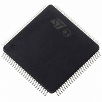
ST10F276Z5T3 STMicroelectronics, ST10F276Z5T3 Datasheet - Page 191

ST10F276Z5T3
Manufacturer Part Number
ST10F276Z5T3
Description
MCU 16BIT 832KBIT FLASH 144-TQFP
Manufacturer
STMicroelectronics
Series
ST10r
Datasheet
1.ST10F276Z5T3.pdf
(239 pages)
Specifications of ST10F276Z5T3
Core Processor
ST10
Core Size
16-Bit
Speed
40MHz
Connectivity
ASC, CAN, EBI/EMI, I²C, SSC, UART/USART
Peripherals
POR, PWM, WDT
Number Of I /o
111
Program Memory Size
832KB (832K x 8)
Program Memory Type
FLASH
Ram Size
68K x 8
Voltage - Supply (vcc/vdd)
4.5 V ~ 5.5 V
Data Converters
A/D 24x10b
Oscillator Type
Internal
Operating Temperature
-40°C ~ 125°C
Package / Case
144-TQFP, 144-VQFP
Cpu Family
ST10
Device Core Size
16b
Frequency (max)
40MHz
Interface Type
CAN/I2C
Total Internal Ram Size
68KB
# I/os (max)
111
Number Of Timers - General Purpose
5
Operating Supply Voltage (typ)
5V
Operating Supply Voltage (max)
5.5V
Operating Supply Voltage (min)
4.5V
On-chip Adc
24-chx10-bit
Instruction Set Architecture
CISC/RISC
Operating Temp Range
-40C to 125C
Operating Temperature Classification
Automotive
Mounting
Surface Mount
Pin Count
144
Package Type
LQFP
Processor Series
ST10F27x
Core
ST10
Data Bus Width
16 bit
Data Ram Size
68 KB
Maximum Clock Frequency
40 MHz
Number Of Programmable I/os
111
Number Of Timers
5
Maximum Operating Temperature
+ 125 C
Mounting Style
SMD/SMT
Minimum Operating Temperature
- 40 C
For Use With
497-6399 - KIT DEV STARTER ST10F276Z5
Lead Free Status / RoHS Status
Lead free / RoHS Compliant
Eeprom Size
-
Lead Free Status / Rohs Status
Compliant
Available stocks
Company
Part Number
Manufacturer
Quantity
Price
Company:
Part Number:
ST10F276Z5T3
Manufacturer:
STMicroelectronics
Quantity:
10 000
ST10F276Z5
23.7.4
23.7.5
Analog reference pins
The accuracy of the A/D converter depends on the accuracy of its analog reference: A noise
in the reference results in proportionate error in a conversion. A low pass filter on the A/D
converter reference source (supplied through pins V
order to clean the signal, minimizing the noise. A simple capacitive bypassing may be suffi-
cient in most cases; in presence of high RF noise energy, inductors or ferrite beads may be
necessary.
In this architecture, V
cuitry of the A/D converter: There is an effective DC current requirement from the reference
voltage by the internal resistor string in the R-C DAC array and by the rest of the analog cir-
cuitry.
An external resistance on V
sons, series resistance is not advisable and more generally, any series devices in the filter
network should be designed to minimize the DC resistance.
Analog input pins
To improve the accuracy of the A/D converter, analog input pins must have low AC imped-
ance. Placing a capacitor with good high frequency characteristics at the input pin of the
device can be effective: The capacitor should be as large as possible, ideally infinite. This
capacitor contributes to attenuating the noise present on the input pin; moreover, its source
charges during the sampling phase, when the analog signal source is a high-impedance
source.
A real filter is typically obtained by using a series resistance with a capacitor on the input pin
(simple RC Filter). The RC filtering may be limited according to the value of source imped-
ance of the transducer or circuit supplying the analog signal to be measured. The filter at the
input pins must be designed taking into account the dynamic characteristics of the input sig-
nal (bandwidth).
Figure 47. A/D converter input pins scheme
V
A
Source
R
R
C
R
R
R
c
C
p
R
S
F
F
L
SW
AD
S
S
EXTERNAL CIRCUIT
AREF
Source impedance
Filter resistance
Filter capacitance
Current limiter resistance
Channel selection switch impedance
Sampling switch impedance
Pin capacitance (two contributions, CP1 and CP2)
Sampling capacitance
and V
AREF
R
Filter
F
C
F
AGND
could introduce error under certain conditions: For this rea-
Current Limiter
pins also represent the power supply of the analog cir-
R
L
C
P1
AREF
and V
V
INTERNAL CIRCUIT SCHEME
DD
AGND
Selection
Channel
Electrical characteristics
R
SW
C
), is recommended in
P2
Sampling
R
AD
C
S
191/239


