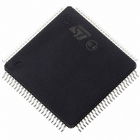
ST10F276Z5T3 STMicroelectronics, ST10F276Z5T3 Datasheet - Page 193

ST10F276Z5T3
Manufacturer Part Number
ST10F276Z5T3
Description
MCU 16BIT 832KBIT FLASH 144-TQFP
Manufacturer
STMicroelectronics
Series
ST10r
Datasheet
1.ST10F276Z5T3.pdf
(239 pages)
Specifications of ST10F276Z5T3
Core Processor
ST10
Core Size
16-Bit
Speed
40MHz
Connectivity
ASC, CAN, EBI/EMI, I²C, SSC, UART/USART
Peripherals
POR, PWM, WDT
Number Of I /o
111
Program Memory Size
832KB (832K x 8)
Program Memory Type
FLASH
Ram Size
68K x 8
Voltage - Supply (vcc/vdd)
4.5 V ~ 5.5 V
Data Converters
A/D 24x10b
Oscillator Type
Internal
Operating Temperature
-40°C ~ 125°C
Package / Case
144-TQFP, 144-VQFP
Cpu Family
ST10
Device Core Size
16b
Frequency (max)
40MHz
Interface Type
CAN/I2C
Total Internal Ram Size
68KB
# I/os (max)
111
Number Of Timers - General Purpose
5
Operating Supply Voltage (typ)
5V
Operating Supply Voltage (max)
5.5V
Operating Supply Voltage (min)
4.5V
On-chip Adc
24-chx10-bit
Instruction Set Architecture
CISC/RISC
Operating Temp Range
-40C to 125C
Operating Temperature Classification
Automotive
Mounting
Surface Mount
Pin Count
144
Package Type
LQFP
Processor Series
ST10F27x
Core
ST10
Data Bus Width
16 bit
Data Ram Size
68 KB
Maximum Clock Frequency
40 MHz
Number Of Programmable I/os
111
Number Of Timers
5
Maximum Operating Temperature
+ 125 C
Mounting Style
SMD/SMT
Minimum Operating Temperature
- 40 C
For Use With
497-6399 - KIT DEV STARTER ST10F276Z5
Lead Free Status / RoHS Status
Lead free / RoHS Compliant
Eeprom Size
-
Lead Free Status / Rohs Status
Compliant
Available stocks
Company
Part Number
Manufacturer
Quantity
Price
Company:
Part Number:
ST10F276Z5T3
Manufacturer:
STMicroelectronics
Quantity:
10 000
ST10F276Z5
In particular two different transient periods can be distinguished (see
1.
2.
The two transients above are not influenced by the voltage source that, due to the presence
of the R
with respect to the ideal source V
respect to the sampling time (T
Figure
Calling f
the anti-aliasing filter, f
least 2f
the conversion period (T
T
S
, which is just a portion of it, even when fixed channel continuous conversion mode is
A first and quick charge transfer from the internal capacitances C
sampling capacitance C
Considering a worst case (since the time constant in reality would be faster) in which
C
C
This relation can again be simplified considering only C
condition. In reality, the transient is faster, but the A/D converter circuitry has been
designed to also be robust in the very worst case: The sampling time T
much longer than the internal time constant:
The charge of C
voltage V
A second charge transfer also involves C
capacitance) through the resistance R
and C
time constant is:
In this case, the time constant depends on the external circuit: In particular, imposing
that the transient is completed well before the end of sampling time T
R
Of course, R
combination with R
definitely bigger than C
charge transfer transient) will be much higher than V
respected (charge balance assuming now C
P2
S
L
49).
0
F
sizing is obtained:
0
, meaning that the constant time of the filter is greater than or at least equal to twice
are in series and the time constant is:
C
is reported in parallel to C
the bandwidth of the source signal (and as a consequence the cut-off frequency of
F
S
filter, cannot provide the extra charge to compensate for the voltage drop on C
were in parallel to C
A1
on the capacitance according to the following equation:
V A2 C S C P1 C P2 C F
L
must also be sized according to the current limitation constraints, in
P1
⋅
(
F
V A1
), according to Nyquist theorem the conversion rate f
and C
S
C
). Again the conversion period T
+
(source impedance) and R
0 τ 2
⋅
⋅
P1
(
S
C S
P2
, C
occurs (C
S
=
+
τ 1
). The filter is typically designed to act as anti-aliasing (see
+
τ 1
P1
is also redistributed on C
τ 2 R L
P2
A
10 R
C P1
; the time constant R
=
P1
<
<
(since the time constant in reality would be faster), the
and C
⋅ L
(
(
R SW
+
R SW
(call C
+
⋅
⋅
S
C P2
(
(
S
C S
is supposed initially completely discharged):
C S
)
+
L
+
, then the final voltage V
=
: Again considering the worst case in which C
P
R AD
R AD
)
V A C F
+
+
F
= C
=
C P1
C P1
(that is typically bigger than the on-chip
⋅
V A
S
)
) C
P1
⋅
•
already charged at V
---------------------- -
C P
+
C P C S
+
+
⋅
F
+ C
V A1
(
C P2
C P2
S
C P1
(filter resistance). Being that C
+
⋅
F
«
P2
C
C S
A1
T
⋅
(
C
S
)
)
F
S
C P1 C P2
), the two capacitances C
+
. The following equation must be
, determining a new value of the
≤
is longer than the sampling time
of the filter is very high with
S
C P2
T S
as an additional worst
+
)
Electrical characteristics
A2
+
Figure
P1
(at the end of the
C S
A1
and C
)
S
):
, a constraint on
S
48):
C
is always
must be at
P2
to the
P
193/239
F
and
is
P2
S


