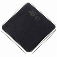
ST10F276Z5T3 STMicroelectronics, ST10F276Z5T3 Datasheet - Page 92

ST10F276Z5T3
Manufacturer Part Number
ST10F276Z5T3
Description
MCU 16BIT 832KBIT FLASH 144-TQFP
Manufacturer
STMicroelectronics
Series
ST10r
Datasheet
1.ST10F276Z5T3.pdf
(239 pages)
Specifications of ST10F276Z5T3
Core Processor
ST10
Core Size
16-Bit
Speed
40MHz
Connectivity
ASC, CAN, EBI/EMI, I²C, SSC, UART/USART
Peripherals
POR, PWM, WDT
Number Of I /o
111
Program Memory Size
832KB (832K x 8)
Program Memory Type
FLASH
Ram Size
68K x 8
Voltage - Supply (vcc/vdd)
4.5 V ~ 5.5 V
Data Converters
A/D 24x10b
Oscillator Type
Internal
Operating Temperature
-40°C ~ 125°C
Package / Case
144-TQFP, 144-VQFP
Cpu Family
ST10
Device Core Size
16b
Frequency (max)
40MHz
Interface Type
CAN/I2C
Total Internal Ram Size
68KB
# I/os (max)
111
Number Of Timers - General Purpose
5
Operating Supply Voltage (typ)
5V
Operating Supply Voltage (max)
5.5V
Operating Supply Voltage (min)
4.5V
On-chip Adc
24-chx10-bit
Instruction Set Architecture
CISC/RISC
Operating Temp Range
-40C to 125C
Operating Temperature Classification
Automotive
Mounting
Surface Mount
Pin Count
144
Package Type
LQFP
Processor Series
ST10F27x
Core
ST10
Data Bus Width
16 bit
Data Ram Size
68 KB
Maximum Clock Frequency
40 MHz
Number Of Programmable I/os
111
Number Of Timers
5
Maximum Operating Temperature
+ 125 C
Mounting Style
SMD/SMT
Minimum Operating Temperature
- 40 C
For Use With
497-6399 - KIT DEV STARTER ST10F276Z5
Lead Free Status / RoHS Status
Lead free / RoHS Compliant
Eeprom Size
-
Lead Free Status / Rohs Status
Compliant
Available stocks
Company
Part Number
Manufacturer
Quantity
Price
Company:
Part Number:
ST10F276Z5T3
Manufacturer:
STMicroelectronics
Quantity:
10 000
Parallel ports
12.2
12.2.1
12.2.2
12.3
92/239
I/Os special features
Open drain mode
Some of the I/O ports of ST10F276Z5 support the open drain capability. This programmable
feature may be used with an external pull-up resistor, in order to get an AND wired logical
function.
This feature is implemented for ports P2, P3, P4, P6, P7 and P8 (see respective sections),
and is controlled through the respective Open Drain Control Registers ODPx.
Input threshold control
The standard inputs of the ST10F276Z5 determine the status of input signals according to
TTL levels. In order to accept and recognize noisy signals, CMOS input thresholds can be
selected instead of the standard TTL thresholds for all the pins. These CMOS thresholds
are defined above the TTL thresholds and feature a higher hysteresis to prevent the inputs
from toggling while the respective input signal level is near the thresholds.
The Port Input Control registers PICON and XPICON are used to select these thresholds for
each Byte of the indicated ports, this means the 8-bit ports P0L, P0H, P1L, P1H, P4, P7 and
P8 are controlled by one bit each while ports P2, P3 and P5 are controlled by two bits each.
All options for individual direction and output mode control are available for each pin,
independent of the selected input threshold.
Alternate port functions
Each port line has one associated programmable alternate input or output function.
●
●
●
●
●
●
If the alternate output function of a pin is to be used, the direction of this pin must be
programmed for output (DPx.y=‘1’), except for some signals that are used directly after reset
and are configured automatically. Otherwise the pin remains in the high-impedance state
and is not effected by the alternate output function. The respective port latch should hold a
PORT0 and PORT1 may be used as address and data lines when accessing external
memory. Besides, PORT1 provides also:
–
–
Port 2, Port 7 and Port 8 are associated with the capture inputs or compare outputs of
the CAPCOM units and/or with the outputs of the PWM0 module, of the PWM1 module
and of the ASC1.
Port 2 is also used for fast external interrupt inputs and for timer 7 input.
Port 3 includes the alternate functions of timers, serial interfaces, the optional bus
control signal BHE and the system clock output (CLKOUT).
Port 4 outputs the additional segment address bit A23...A16 in systems where more
than 64 Kbytes of memory are to be access directly. In addition, CAN1, CAN2 and I
lines are provided.
Port 5 is used as analog input channels of the A/D converter or as timer control signals.
Port 6 provides optional bus arbitration signals (BREQ, HLDA, HOLD) and chip select
signals and the SSC1 lines.
Input capture lines
8 additional analog input channels to the A/D converter
ST10F276Z5
2
C


