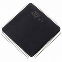
ST10F276Z5T3 STMicroelectronics, ST10F276Z5T3 Datasheet - Page 77

ST10F276Z5T3
Manufacturer Part Number
ST10F276Z5T3
Description
MCU 16BIT 832KBIT FLASH 144-TQFP
Manufacturer
STMicroelectronics
Series
ST10r
Datasheet
1.ST10F276Z5T3.pdf
(239 pages)
Specifications of ST10F276Z5T3
Core Processor
ST10
Core Size
16-Bit
Speed
40MHz
Connectivity
ASC, CAN, EBI/EMI, I²C, SSC, UART/USART
Peripherals
POR, PWM, WDT
Number Of I /o
111
Program Memory Size
832KB (832K x 8)
Program Memory Type
FLASH
Ram Size
68K x 8
Voltage - Supply (vcc/vdd)
4.5 V ~ 5.5 V
Data Converters
A/D 24x10b
Oscillator Type
Internal
Operating Temperature
-40°C ~ 125°C
Package / Case
144-TQFP, 144-VQFP
Cpu Family
ST10
Device Core Size
16b
Frequency (max)
40MHz
Interface Type
CAN/I2C
Total Internal Ram Size
68KB
# I/os (max)
111
Number Of Timers - General Purpose
5
Operating Supply Voltage (typ)
5V
Operating Supply Voltage (max)
5.5V
Operating Supply Voltage (min)
4.5V
On-chip Adc
24-chx10-bit
Instruction Set Architecture
CISC/RISC
Operating Temp Range
-40C to 125C
Operating Temperature Classification
Automotive
Mounting
Surface Mount
Pin Count
144
Package Type
LQFP
Processor Series
ST10F27x
Core
ST10
Data Bus Width
16 bit
Data Ram Size
68 KB
Maximum Clock Frequency
40 MHz
Number Of Programmable I/os
111
Number Of Timers
5
Maximum Operating Temperature
+ 125 C
Mounting Style
SMD/SMT
Minimum Operating Temperature
- 40 C
For Use With
497-6399 - KIT DEV STARTER ST10F276Z5
Lead Free Status / RoHS Status
Lead free / RoHS Compliant
Eeprom Size
-
Lead Free Status / Rohs Status
Compliant
Available stocks
Company
Part Number
Manufacturer
Quantity
Price
Company:
Part Number:
ST10F276Z5T3
Manufacturer:
STMicroelectronics
Quantity:
10 000
ST10F276Z5
7
External bus controller
All of the external memory accesses are performed by the on-chip external bus controller.
The EBC can be programmed to single chip mode when no external memory is required, or
to one of four different external memory access modes:
●
●
●
●
In demultiplexed bus modes addresses are output on PORT1 and data is input / output on
PORT0 or P0L, respectively. In the multiplexed bus modes both addresses and data use
PORT0 for input / output.
Timing characteristics of the external bus interface (memory cycle time, memory tri-state
time, length of ALE and read / write delay) are programmable giving the choice of a wide
range of memories and external peripherals.
Up to four independent address windows may be defined (using register pairs ADDRSELx /
BUSCONx) to access different resources and bus characteristics.
These address windows are arranged hierarchically where BUSCON4 overrides BUSCON3
and BUSCON2 overrides BUSCON1.
All accesses to locations not covered by these four address windows are controlled by
BUSCON0. Up to five external CS signals (four windows plus default) can be generated in
order to save external glue logic. Access to very slow memories is supported by a ‘Ready’
function.
A HOLD / HLDA protocol is available for bus arbitration which shares external resources
with other bus masters.
The bus arbitration is enabled by setting bit HLDEN in register PSW. After setting HLDEN
once, pins P6.7...P6.5 (BREQ, HLDA, HOLD) are automatically controlled by the EBC. In
master mode (default after reset) the HLDA pin is an output. By setting bit DP6.7 to’1’ the
slave mode is selected where pin HLDA is switched to input. This directly connects the slave
controller to another master controller without glue logic.
For applications which require less external memory space, the address space can be
restricted to 1 Mbyte, 256 Kbytes or to 64 Kbytes. Port 4 outputs all eight address lines if an
address space of 16M Bytes is used, otherwise four, two or no address lines.
Chip select timing can be made programmable. By default (after reset), the CSx lines
change half a CPU clock cycle after the rising edge of ALE. With the CSCFG bit set in the
SYSCON register the CSx lines change with the rising edge of ALE.
The active level of the READY pin can be set by bit RDYPOL in the BUSCONx registers.
When the READY function is enabled for a specific address window, each bus cycle within
the window must be terminated with the active level defined by bit RDYPOL in the
associated BUSCON register.
16- / 18- / 20- / 24-bit addresses and 16-bit data, demultiplexed
16- / 18- / 20- / 24-bit addresses and 16-bit data, multiplexed
16- / 18- / 20- / 24-bit addresses and 8-bit data, multiplexed
16- / 18- / 20- / 24-bit addresses and 8-bit data, demultiplexed
External bus controller
77/239


