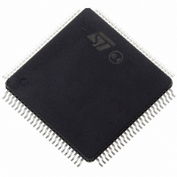
ST10F276Z5T3 STMicroelectronics, ST10F276Z5T3 Datasheet - Page 40

ST10F276Z5T3
Manufacturer Part Number
ST10F276Z5T3
Description
MCU 16BIT 832KBIT FLASH 144-TQFP
Manufacturer
STMicroelectronics
Series
ST10r
Datasheet
1.ST10F276Z5T3.pdf
(239 pages)
Specifications of ST10F276Z5T3
Core Processor
ST10
Core Size
16-Bit
Speed
40MHz
Connectivity
ASC, CAN, EBI/EMI, I²C, SSC, UART/USART
Peripherals
POR, PWM, WDT
Number Of I /o
111
Program Memory Size
832KB (832K x 8)
Program Memory Type
FLASH
Ram Size
68K x 8
Voltage - Supply (vcc/vdd)
4.5 V ~ 5.5 V
Data Converters
A/D 24x10b
Oscillator Type
Internal
Operating Temperature
-40°C ~ 125°C
Package / Case
144-TQFP, 144-VQFP
Cpu Family
ST10
Device Core Size
16b
Frequency (max)
40MHz
Interface Type
CAN/I2C
Total Internal Ram Size
68KB
# I/os (max)
111
Number Of Timers - General Purpose
5
Operating Supply Voltage (typ)
5V
Operating Supply Voltage (max)
5.5V
Operating Supply Voltage (min)
4.5V
On-chip Adc
24-chx10-bit
Instruction Set Architecture
CISC/RISC
Operating Temp Range
-40C to 125C
Operating Temperature Classification
Automotive
Mounting
Surface Mount
Pin Count
144
Package Type
LQFP
Processor Series
ST10F27x
Core
ST10
Data Bus Width
16 bit
Data Ram Size
68 KB
Maximum Clock Frequency
40 MHz
Number Of Programmable I/os
111
Number Of Timers
5
Maximum Operating Temperature
+ 125 C
Mounting Style
SMD/SMT
Minimum Operating Temperature
- 40 C
For Use With
497-6399 - KIT DEV STARTER ST10F276Z5
Lead Free Status / RoHS Status
Lead free / RoHS Compliant
Eeprom Size
-
Lead Free Status / Rohs Status
Compliant
Available stocks
Company
Part Number
Manufacturer
Quantity
Price
Company:
Part Number:
ST10F276Z5T3
Manufacturer:
STMicroelectronics
Quantity:
10 000
Internal Flash memory
4.5.6
4.5.7
40/239
Flash non volatile access protection register 0
Due to ST10 architecture, the XFLASH is seen as external memory: this made impossible to
access protect it from real external memory or internal RAM.
FNVAPR0 (0x0E DFB8)
Table 24.
Flash non volatile access protection register 1 low
FNVAPR1L (0x0E DFBC)
Table 25.
PDS15 PDS14 PDS13 PDS12 PDS11 PDS10 PDS9 PDS8 PDS7 PDS6 PDS5 PDS4 PDS3 PDS2 PDS1 PDS0
RW
15
15
PDS(15:0)
DBGP
ACCP
Bit
Bit
RW
14
14
RW
Flash non volatile access protection register 0
Flash non volatile access protection register 1 low
13
13
Access Protection
This bit, if programmed at 0, disables any access (read/write) to data mapped inside
IFlash Module address space, unless the current instruction is fetched from one of the
two Flash modules.
Debug Protection
This bit, if erased at 1, allows to by-pass all the protections using the Debug features
through the Test Interface. If programmed at 0, on the contrary, all the debug features,
the Test Interface and all the Flash Test modes are disabled. Even STMicroelectronics
will not be able to access the device to run any eventual failure analysis.
Protections Disable 15-0
If bit PDSx is programmed at 0 and bit PENx is erased at 1, the action of bit ACCP is
disabled. Bit PDS0 can be programmed at 0 only if bits DBGP and ACCP have already
been programmed at 0. Bit PDSx can be programmed at 0 only if bit PENx-1 has
already been programmed at 0.
RW
12
12
RW
11
11
RW
10
10
RW
reserved
9
9
NVR
NVR
RW
8
8
RW
7
Function
7
Function
RW
6
6
RW
5
5
RW
4
4
RW
3
3
Delivery value: ACFFh
Delivery value: FFFFh
RW
2
2
ST10F276Z5
DBGP
RW
RW
1
1
ACCP
RW
RW
0
0


