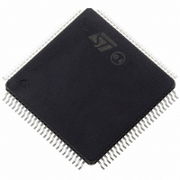
ST10F276Z5T3 STMicroelectronics, ST10F276Z5T3 Datasheet - Page 215

ST10F276Z5T3
Manufacturer Part Number
ST10F276Z5T3
Description
MCU 16BIT 832KBIT FLASH 144-TQFP
Manufacturer
STMicroelectronics
Series
ST10r
Datasheet
1.ST10F276Z5T3.pdf
(239 pages)
Specifications of ST10F276Z5T3
Core Processor
ST10
Core Size
16-Bit
Speed
40MHz
Connectivity
ASC, CAN, EBI/EMI, I²C, SSC, UART/USART
Peripherals
POR, PWM, WDT
Number Of I /o
111
Program Memory Size
832KB (832K x 8)
Program Memory Type
FLASH
Ram Size
68K x 8
Voltage - Supply (vcc/vdd)
4.5 V ~ 5.5 V
Data Converters
A/D 24x10b
Oscillator Type
Internal
Operating Temperature
-40°C ~ 125°C
Package / Case
144-TQFP, 144-VQFP
Cpu Family
ST10
Device Core Size
16b
Frequency (max)
40MHz
Interface Type
CAN/I2C
Total Internal Ram Size
68KB
# I/os (max)
111
Number Of Timers - General Purpose
5
Operating Supply Voltage (typ)
5V
Operating Supply Voltage (max)
5.5V
Operating Supply Voltage (min)
4.5V
On-chip Adc
24-chx10-bit
Instruction Set Architecture
CISC/RISC
Operating Temp Range
-40C to 125C
Operating Temperature Classification
Automotive
Mounting
Surface Mount
Pin Count
144
Package Type
LQFP
Processor Series
ST10F27x
Core
ST10
Data Bus Width
16 bit
Data Ram Size
68 KB
Maximum Clock Frequency
40 MHz
Number Of Programmable I/os
111
Number Of Timers
5
Maximum Operating Temperature
+ 125 C
Mounting Style
SMD/SMT
Minimum Operating Temperature
- 40 C
For Use With
497-6399 - KIT DEV STARTER ST10F276Z5
Lead Free Status / RoHS Status
Lead free / RoHS Compliant
Eeprom Size
-
Lead Free Status / Rohs Status
Compliant
Available stocks
Company
Part Number
Manufacturer
Quantity
Price
Company:
Part Number:
ST10F276Z5T3
Manufacturer:
STMicroelectronics
Quantity:
10 000
ST10F276Z5
Table 107. Demultiplexed bus (continued)
1. RW-delay and
2. Read data is latched with the same clock edge that triggers the address change and the rising RD edge.
1
The following figures
memory cycle.
t
t
t
t
t
t
t
t
t
t
t
t
t
t
t
Symbol
38
39
41
82
83
46
47
48
49
50
51
53
68
55
57
Therefore address changes which occur before the end of RD have no impact on read cycles.
Partially tested, guaranteed by design characterization.
CC
SR
CC
CC
CC
SR
SR
CC
CC
CC Data valid to WrCS
SR Data hold after RdCS
SR
SR
CC
CC Data hold after WrCS
ALE falling edge to
Latched CS
Latched CS low to
Valid Data In
Latched CS hold after
RD, WR
Address setup to
RdCS, WrCS
(with RW-delay)
Address setup to
RdCS, WrCS
(no RW-delay)
RdCS to Valid Data In
(with RW-delay)
RdCS to Valid Data In
(no RW-delay)
RdCS, WrCS low time
(with RW-delay)
RdCS, WrCS low time
(no RW-delay)
Data float after RdCS
(with RW-delay)
Data float after RdCS
(no RW-delay)
Address hold after
RdCS, WrCS
t
A
Parameter
refer to the next following bus cycle.
(Figure 57
to
– 8.5 + t
15.5 + t
14 + 2t
– 4 – t
2 + 2t
28 + t
10 + t
Figure
2 + t
2 + t
Min.
F
TCL = 12.5 ns
–
–
–
0
–
–
CPU
F
F
A
C
C
A
A
C
F
64) present the different configurations of external
= 40 MHz
16.5 + t
16.5 + t
16.5 + t
4 + t
6 – t
4 + t
Max.
2t
–
–
–
–
–
–
–
–
–
A
A
C
F
C
C
F
+
2TCL – 9.5 + t
3TCL – 9.5 + t
TCL – 10.5 + t
TCL – 10.5 + t
2TCL – 15 + t
2TCL – 11 +
TCL –10.5 +
– 8.5 + t
– 4 – t
1/2 TCL = 1 to 64 MHz
Min.
2t
2t
Variable CPU clock
–
–
–
0
–
–
A
A
Electrical characteristics
A
F
C
F
C
C
F
3TCL – 21+ t
2TCL – 8.5 + t
2TCL – 21 + t
3TCL – 21 + t
TCL – 8.5 + t
6 – t
Max.
2t
–
–
–
–
–
–
–
–
–
A
A
C
F
215/239
C
C
+
F
ns
ns
ns
ns
ns
ns
ns
ns
ns
ns
ns
ns
ns
ns
ns


