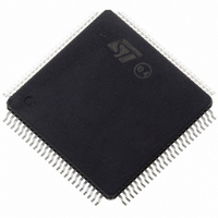
ST10F276Z5T3 STMicroelectronics, ST10F276Z5T3 Datasheet - Page 53

ST10F276Z5T3
Manufacturer Part Number
ST10F276Z5T3
Description
MCU 16BIT 832KBIT FLASH 144-TQFP
Manufacturer
STMicroelectronics
Series
ST10r
Datasheet
1.ST10F276Z5T3.pdf
(239 pages)
Specifications of ST10F276Z5T3
Core Processor
ST10
Core Size
16-Bit
Speed
40MHz
Connectivity
ASC, CAN, EBI/EMI, I²C, SSC, UART/USART
Peripherals
POR, PWM, WDT
Number Of I /o
111
Program Memory Size
832KB (832K x 8)
Program Memory Type
FLASH
Ram Size
68K x 8
Voltage - Supply (vcc/vdd)
4.5 V ~ 5.5 V
Data Converters
A/D 24x10b
Oscillator Type
Internal
Operating Temperature
-40°C ~ 125°C
Package / Case
144-TQFP, 144-VQFP
Cpu Family
ST10
Device Core Size
16b
Frequency (max)
40MHz
Interface Type
CAN/I2C
Total Internal Ram Size
68KB
# I/os (max)
111
Number Of Timers - General Purpose
5
Operating Supply Voltage (typ)
5V
Operating Supply Voltage (max)
5.5V
Operating Supply Voltage (min)
4.5V
On-chip Adc
24-chx10-bit
Instruction Set Architecture
CISC/RISC
Operating Temp Range
-40C to 125C
Operating Temperature Classification
Automotive
Mounting
Surface Mount
Pin Count
144
Package Type
LQFP
Processor Series
ST10F27x
Core
ST10
Data Bus Width
16 bit
Data Ram Size
68 KB
Maximum Clock Frequency
40 MHz
Number Of Programmable I/os
111
Number Of Timers
5
Maximum Operating Temperature
+ 125 C
Mounting Style
SMD/SMT
Minimum Operating Temperature
- 40 C
For Use With
497-6399 - KIT DEV STARTER ST10F276Z5
Lead Free Status / RoHS Status
Lead free / RoHS Compliant
Eeprom Size
-
Lead Free Status / Rohs Status
Compliant
Available stocks
Company
Part Number
Manufacturer
Quantity
Price
Company:
Part Number:
ST10F276Z5T3
Manufacturer:
STMicroelectronics
Quantity:
10 000
ST10F276Z5
5.2.6
Figure 8.
1. As long as the device is in BSL, the user’s software should not try to execute code from the internal IFlash,
Loading the start-up code
After the serial link initialization sequence (see following chapters), the BSL enters a loop to
receive 32 bytes (boot via UART) or 128 bytes (boot via CAN).
These bytes are stored sequentially into the device Dual-Port RAM from location 00’FA40h.
To execute the loaded code, the BSL then jumps to location 00’FA40h. The bootstrap
sequence running from the Test-Flash is now terminated; however, the microcontroller
remains in BSL mode.
Most probably, the initially loaded routine, being the first level user code, will load additional
code and data. This first level user code may use the pre-initialized interface (UART or CAN)
to receive data and a second level of code, and store it in arbitrary user-defined locations.
This second level of code may be
●
●
●
In all cases, the device still runs in BSL mode, that is, with the watchdog timer disabled and
limited access to the internal IFLASH area.
BSL mode active
EA pin
Code fetch from
internal FLASH area
Data fetch from
internal FLASH area
as the fetches are redirected to the Test-Flash.
The final application code
Another, more sophisticated, loader routine that adds a transmission protocol to
enhance the integrity of the loaded code or data
A code sequence to change the system configuration and enable the bus interface to
store the received data into external memory
Memory configuration after reset
Yes (P0L.4 = ‘0’)
High
Test-FLASH access
User IFLASH access
16 Mbytes
RAM
int.
0
1
access to
int. FLASH
enabled
access to
external
bus
disabled
Yes (P0L.4 = ‘0’)
Low
Test-FLASH access
User IFLASH access
16 Mbytes
RAM
int.
0
1
access to
int. FLASH
enabled
access to
external
bus
enabled
No (P0L.4 = ‘1’)
According to application
User IFLASH access
User IFLASH access
16 Mbytes
RAM
int.
Bootstrap loader
0
1
Depends on
reset config.
(EA, P0)
Depends on
reset config.
53/239


