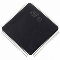
ST10F276Z5T3 STMicroelectronics, ST10F276Z5T3 Datasheet - Page 194

ST10F276Z5T3
Manufacturer Part Number
ST10F276Z5T3
Description
MCU 16BIT 832KBIT FLASH 144-TQFP
Manufacturer
STMicroelectronics
Series
ST10r
Datasheet
1.ST10F276Z5T3.pdf
(239 pages)
Specifications of ST10F276Z5T3
Core Processor
ST10
Core Size
16-Bit
Speed
40MHz
Connectivity
ASC, CAN, EBI/EMI, I²C, SSC, UART/USART
Peripherals
POR, PWM, WDT
Number Of I /o
111
Program Memory Size
832KB (832K x 8)
Program Memory Type
FLASH
Ram Size
68K x 8
Voltage - Supply (vcc/vdd)
4.5 V ~ 5.5 V
Data Converters
A/D 24x10b
Oscillator Type
Internal
Operating Temperature
-40°C ~ 125°C
Package / Case
144-TQFP, 144-VQFP
Cpu Family
ST10
Device Core Size
16b
Frequency (max)
40MHz
Interface Type
CAN/I2C
Total Internal Ram Size
68KB
# I/os (max)
111
Number Of Timers - General Purpose
5
Operating Supply Voltage (typ)
5V
Operating Supply Voltage (max)
5.5V
Operating Supply Voltage (min)
4.5V
On-chip Adc
24-chx10-bit
Instruction Set Architecture
CISC/RISC
Operating Temp Range
-40C to 125C
Operating Temperature Classification
Automotive
Mounting
Surface Mount
Pin Count
144
Package Type
LQFP
Processor Series
ST10F27x
Core
ST10
Data Bus Width
16 bit
Data Ram Size
68 KB
Maximum Clock Frequency
40 MHz
Number Of Programmable I/os
111
Number Of Timers
5
Maximum Operating Temperature
+ 125 C
Mounting Style
SMD/SMT
Minimum Operating Temperature
- 40 C
For Use With
497-6399 - KIT DEV STARTER ST10F276Z5
Lead Free Status / RoHS Status
Lead free / RoHS Compliant
Eeprom Size
-
Lead Free Status / Rohs Status
Compliant
Available stocks
Company
Part Number
Manufacturer
Quantity
Price
Company:
Part Number:
ST10F276Z5T3
Manufacturer:
STMicroelectronics
Quantity:
10 000
Electrical characteristics
194/239
selected (fastest conversion rate at a specific channel): In conclusion, it is evident that the
time constant of the filter R
charge level on C
the sampling switch is closed.
Figure 49. Anti-aliasing filter and conversion rate
The considerations above lead to impose new constraints to the external circuit, to reduce
the accuracy error due to the voltage drop on C
above, it is simple to derive the following relation between the ideal and real sampled volt-
age on C
From this formula, in the worst case (when V
ing to accept a maximum error of half a count (~2.44mV), it is immediately evident that a
constraint is on C
The next section provides an example of how to design the external network, based on
some reasonable values for the internal parameters and on a hypothesis on the characteris-
tics of the analog signal to be sampled.
Anti-aliasing filter (f
Analog source bandwidth (V
S
:
f
f
0
F
F
S
F
= RC Filter pole)
value:
cannot be modified by the analog signal source during the time in which
Noise
f
f
A
F
)
C
F
-----------
V A2
is definitely much higher than the sampling time T
V A
=
Sampled signal spectrum (f
------------------------------------------------------------
C P1
TC ≤ 2 RFCF (Conversion rate vs. filter pole)
f
2 f0 ≤ fC (Nyquist)
C F 2048 C S
F
= f
C P1
0
>
+
(Anti-aliasing Filtering Condition)
A
C P2
+
f
is maximum, that is for instance 5 V), assum-
0
C P2
S
; from the two charge balance equations
+
⋅
C F
+
C F
+
C S
C
= conversion Rate)
f
C
f
ST10F276Z5
S
, so the


