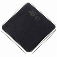
ST10F276Z5T3 STMicroelectronics, ST10F276Z5T3 Datasheet - Page 192

ST10F276Z5T3
Manufacturer Part Number
ST10F276Z5T3
Description
MCU 16BIT 832KBIT FLASH 144-TQFP
Manufacturer
STMicroelectronics
Series
ST10r
Datasheet
1.ST10F276Z5T3.pdf
(239 pages)
Specifications of ST10F276Z5T3
Core Processor
ST10
Core Size
16-Bit
Speed
40MHz
Connectivity
ASC, CAN, EBI/EMI, I²C, SSC, UART/USART
Peripherals
POR, PWM, WDT
Number Of I /o
111
Program Memory Size
832KB (832K x 8)
Program Memory Type
FLASH
Ram Size
68K x 8
Voltage - Supply (vcc/vdd)
4.5 V ~ 5.5 V
Data Converters
A/D 24x10b
Oscillator Type
Internal
Operating Temperature
-40°C ~ 125°C
Package / Case
144-TQFP, 144-VQFP
Cpu Family
ST10
Device Core Size
16b
Frequency (max)
40MHz
Interface Type
CAN/I2C
Total Internal Ram Size
68KB
# I/os (max)
111
Number Of Timers - General Purpose
5
Operating Supply Voltage (typ)
5V
Operating Supply Voltage (max)
5.5V
Operating Supply Voltage (min)
4.5V
On-chip Adc
24-chx10-bit
Instruction Set Architecture
CISC/RISC
Operating Temp Range
-40C to 125C
Operating Temperature Classification
Automotive
Mounting
Surface Mount
Pin Count
144
Package Type
LQFP
Processor Series
ST10F27x
Core
ST10
Data Bus Width
16 bit
Data Ram Size
68 KB
Maximum Clock Frequency
40 MHz
Number Of Programmable I/os
111
Number Of Timers
5
Maximum Operating Temperature
+ 125 C
Mounting Style
SMD/SMT
Minimum Operating Temperature
- 40 C
For Use With
497-6399 - KIT DEV STARTER ST10F276Z5
Lead Free Status / RoHS Status
Lead free / RoHS Compliant
Eeprom Size
-
Lead Free Status / Rohs Status
Compliant
Available stocks
Company
Part Number
Manufacturer
Quantity
Price
Company:
Part Number:
ST10F276Z5T3
Manufacturer:
STMicroelectronics
Quantity:
10 000
Electrical characteristics
192/239
Input leakage and external circuit
The series resistor utilized to limit the current to a pin (see R
with a large source impedance, can lead to a degradation of A/D converter accuracy when
input leakage is present.
Data about maximum input leakage current at each pin is provided in the datasheet (Electri-
cal Characteristics section). Input leakage is greatest at high operating temperatures and in
general decreases by one half for each 10° C decrease in temperature.
Considering that, for a 10-bit A/D converter one count is about 5mV (assuming V
5 V), an input leakage of 100nA acting though an R
an error of exactly one count (5mV); if the resistance were 100kΩ, the error would become
two counts.
Eventual additional leakage due to external clamping diodes must also be taken into
account in computing the total leakage affecting the A/D converter measurements. Another
contribution to the total leakage is represented by the charge sharing effects with the sam-
pling capacitance: C
the conversion rate of a single channel (maximum when fixed channel continuous conver-
sion mode is selected), it can be seen as a resistive path to ground. For instance, assuming
a conversion rate of 250 kHz, with C
1 / f
the error induced by the voltage partitioning between this resistance (sampled voltage on
C
respect the following relation:
The formula above places constraints on external network design, in particular on resistive
path.
A second aspect involving the capacitance network must be considered. Assuming the three
capacitances C
equivalent circuit shown in
close), a charge sharing phenomena is installed.
Figure 48. Charge sharing timing diagram during sampling phase
S
) and the sum of R
C
C
S
, where f
V
V
V
V
CS
A
A2
A1
F
, C
C
1
represents the conversion rate at the considered channel). To minimize
P1
S
S
and C
Voltage Transient on C
being substantially a switched capacitance, with a frequency equal to
+ R
V A
F
Figure
P2
+ R
2
⋅
R S
----------------------------------------------------------------------------- -
are initially charged at the source voltage V
L
+
+ R
47), when the sampling phase is started (A/D switch
R F
S
SW
equal to 4 pF, a resistance of 1MΩ is obtained (R
+
S
R L
+ R
R EQ
+
AD
R SW
T
S
, the external circuit must be designed to
∆V < 0.5 LSB
+
t
L
R AD
= 50kΩ of external resistance leads to
<
τ
τ
1
2
1
-- - LSB
2
L
< (R
= R
in
L
SW
Figure
(C
S
+ R
+ C
AD
P1
47), in combination
) C
+ C
S
A
<< T
P2
(refer to the
)
ST10F276Z5
S
AREF
=
EQ
=


