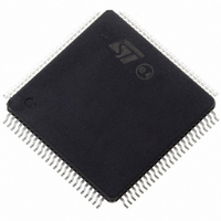
ST10F276Z5T3 STMicroelectronics, ST10F276Z5T3 Datasheet - Page 183

ST10F276Z5T3
Manufacturer Part Number
ST10F276Z5T3
Description
MCU 16BIT 832KBIT FLASH 144-TQFP
Manufacturer
STMicroelectronics
Series
ST10r
Datasheet
1.ST10F276Z5T3.pdf
(239 pages)
Specifications of ST10F276Z5T3
Core Processor
ST10
Core Size
16-Bit
Speed
40MHz
Connectivity
ASC, CAN, EBI/EMI, I²C, SSC, UART/USART
Peripherals
POR, PWM, WDT
Number Of I /o
111
Program Memory Size
832KB (832K x 8)
Program Memory Type
FLASH
Ram Size
68K x 8
Voltage - Supply (vcc/vdd)
4.5 V ~ 5.5 V
Data Converters
A/D 24x10b
Oscillator Type
Internal
Operating Temperature
-40°C ~ 125°C
Package / Case
144-TQFP, 144-VQFP
Cpu Family
ST10
Device Core Size
16b
Frequency (max)
40MHz
Interface Type
CAN/I2C
Total Internal Ram Size
68KB
# I/os (max)
111
Number Of Timers - General Purpose
5
Operating Supply Voltage (typ)
5V
Operating Supply Voltage (max)
5.5V
Operating Supply Voltage (min)
4.5V
On-chip Adc
24-chx10-bit
Instruction Set Architecture
CISC/RISC
Operating Temp Range
-40C to 125C
Operating Temperature Classification
Automotive
Mounting
Surface Mount
Pin Count
144
Package Type
LQFP
Processor Series
ST10F27x
Core
ST10
Data Bus Width
16 bit
Data Ram Size
68 KB
Maximum Clock Frequency
40 MHz
Number Of Programmable I/os
111
Number Of Timers
5
Maximum Operating Temperature
+ 125 C
Mounting Style
SMD/SMT
Minimum Operating Temperature
- 40 C
For Use With
497-6399 - KIT DEV STARTER ST10F276Z5
Lead Free Status / RoHS Status
Lead free / RoHS Compliant
Eeprom Size
-
Lead Free Status / Rohs Status
Compliant
Available stocks
Company
Part Number
Manufacturer
Quantity
Price
Company:
Part Number:
ST10F276Z5T3
Manufacturer:
STMicroelectronics
Quantity:
10 000
ST10F276Z5
Table 92.
1. This specification is not valid for outputs which are switched to open drain mode. In this case the
2. Port 5 leakage values are granted for not selected A/D converter channel. One channels is always
3. The leakage of P2.0 is higher than other pins due to the additional logic (pass gates active only in specific
4. Not 100% tested, guaranteed by design characterization.
5. Overload conditions occur if the standard operating conditions are exceeded, that is, the voltage on any
6. This specification is only valid during Reset, or during Hold- or Adapt-mode. Port 6 pins are only affected if
7. The maximum current may be drawn while the respective signal line remains inactive.
8. The minimum current must be drawn in order to drive the respective signal line active.
9. The power supply currents, I
10. The Idle mode supply current is a function of the operating frequency (f
11. This parameter is tested including leakage currents. All inputs (including pins configured as inputs) at 0 to
I
I
SB2
SB3
Symbol
respective output floats and the voltage is imposed by the external circuitry.
selected (by default, after reset, P5.0 is selected). For the selected channel the leakage value is similar to
that of other port pins.
test modes) implemented on input path. Pay attention to not stress P2.0 input pin with negative overload
beyond the specified limits: Failures in Flash reading may occur (sense amplifier perturbation). Refer to
next
pin exceeds the specified range (that is, V
overload currents on all port pins may not exceed 50 mA. The supply voltage must remain within the
specified limits.
they are used for CS output and the open drain function is not enabled.
MHz). This dependency is illustrated in the
at maximum CPU clock frequency with all outputs disconnected and all inputs at V
V
- Fetching code from IRAM and XRAM1 (for I
accessing in read and write to both XRAM modules
- Watchdog Timer is enabled and regularly serviced
- RTC is running with main oscillator clock as reference, generating a tick interrupts every 192 clock cycles
- Four channels of XPWM are running (waves period: 2, 2.5, 3 and 4 CPU clock cycles): No output toggling
- Five General Purpose Timers are running in timer mode with prescaler equal to 8 (T2, T3, T4, T5, T6)
- ADC is in Auto Scan Continuous Conversion mode on all 16 channels of Port5
- All interrupts generated by XPWM, RTC, Timers and ADC are not serviced
dependency is illustrated in the Figure 44 below. These parameters are tested and at maximum CPU clock
with all outputs disconnected and all inputs at V
0.1 V or at V
disconnected. Furthermore, the Main Voltage Regulator is assumed off: In case it is not, additional 1mA
shall be assumed.
IH1min
Figure 44
: This implies I/O current is not considered. The device performs the following actions:
Standby supply current
(RTC on, 32 kHz Oscillator on,
main VDD off, VSTBY on)
Standby supply current
(VDD transient condition)
DC characteristics (continued)
DD
for a scheme of the input circuitry.
– 0.1 V to V
Parameter
DD
CC1
, V
and I
AREF
CC2
(11)
(4) (11)
= 0 V, all outputs (including pins configured as outputs)
, are function of the operating frequency (f
OV
Figure 45
CC1
> V
IL
DD
) or from all sectors of both IFlash and XFlash (for I
or V
+ 0.3 V or V
V
T
V
T
Test Condition
A
A
below. These parameters are tested at V
IH
STBY
STBY
= 25 °C
= 125 °C
, RSTIN pin at V
= 5.5 V
= 5.5 V
–
OV
< –0.3 V). The absolute sum of input
CPU
IH1min
is expressed in MHz). This
Min.
Electrical characteristics
.
–
–
–
Limit values
IL
CPU
or V
is expressed in
IH
Max.
, RSTIN pin at
250
500
2.5
DDmax
CC2
and
183/239
Unit
mA
µA
µA
),


