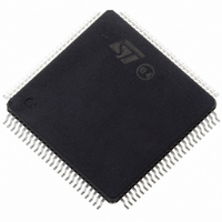
ST10F276Z5T3 STMicroelectronics, ST10F276Z5T3 Datasheet - Page 22

ST10F276Z5T3
Manufacturer Part Number
ST10F276Z5T3
Description
MCU 16BIT 832KBIT FLASH 144-TQFP
Manufacturer
STMicroelectronics
Series
ST10r
Datasheet
1.ST10F276Z5T3.pdf
(239 pages)
Specifications of ST10F276Z5T3
Core Processor
ST10
Core Size
16-Bit
Speed
40MHz
Connectivity
ASC, CAN, EBI/EMI, I²C, SSC, UART/USART
Peripherals
POR, PWM, WDT
Number Of I /o
111
Program Memory Size
832KB (832K x 8)
Program Memory Type
FLASH
Ram Size
68K x 8
Voltage - Supply (vcc/vdd)
4.5 V ~ 5.5 V
Data Converters
A/D 24x10b
Oscillator Type
Internal
Operating Temperature
-40°C ~ 125°C
Package / Case
144-TQFP, 144-VQFP
Cpu Family
ST10
Device Core Size
16b
Frequency (max)
40MHz
Interface Type
CAN/I2C
Total Internal Ram Size
68KB
# I/os (max)
111
Number Of Timers - General Purpose
5
Operating Supply Voltage (typ)
5V
Operating Supply Voltage (max)
5.5V
Operating Supply Voltage (min)
4.5V
On-chip Adc
24-chx10-bit
Instruction Set Architecture
CISC/RISC
Operating Temp Range
-40C to 125C
Operating Temperature Classification
Automotive
Mounting
Surface Mount
Pin Count
144
Package Type
LQFP
Processor Series
ST10F27x
Core
ST10
Data Bus Width
16 bit
Data Ram Size
68 KB
Maximum Clock Frequency
40 MHz
Number Of Programmable I/os
111
Number Of Timers
5
Maximum Operating Temperature
+ 125 C
Mounting Style
SMD/SMT
Minimum Operating Temperature
- 40 C
For Use With
497-6399 - KIT DEV STARTER ST10F276Z5
Lead Free Status / RoHS Status
Lead free / RoHS Compliant
Eeprom Size
-
Lead Free Status / Rohs Status
Compliant
Available stocks
Company
Part Number
Manufacturer
Quantity
Price
Company:
Part Number:
ST10F276Z5T3
Manufacturer:
STMicroelectronics
Quantity:
10 000
Pin data
Table 2.
22/239
P0H.1 - P0H.7
P1H.0 - P1H.7
P0L.0 -P0L.7,
P1L.0 - P1L.7
EA / V
Symbol
P0H.0
STBY
Pin description (continued)
100-107,
111-117
118-125
128-135
108,
132
133
134
135
Pin
99
Type
I/O
I/O
I
I
I
I
I
External access enable pin.
A low level applied to this pin during and after Reset forces the ST10F276Z5 to
start the program from the external memory space. A high level forces the
ST10F276Z5 to start in the internal memory space. This pin is also used (when
Standby mode is entered, that is the device under reset and main V
off) to bias the 32 kHz oscillator amplifier circuit and to provide a reference
voltage for the low-power embedded voltage regulator which generates the
internal 1.8 V supply for the RTC module (when not disabled) and to retain data
inside the Standby portion of the XRAM (16Kbyte).
It can range from 4.5 to 5.5 V (6 V for a reduced amount of time during the
device life, 4.0 V when RTC and 32 kHz on-chip oscillator amplifier are turned
off). In running mode, this pin can be tied low during reset without affecting 32
kHz oscillator, RTC and XRAM activities, since the presence of a stable V
guarantees the proper biasing of all those modules.
Two 8-bit bidirectional I/O ports P0L and P0H, bit-wise programmable for input or
output via direction bit. Programming an I/O pin as input forces the
corresponding output driver to high impedance state. The input threshold of
Port 0 is selectable (TTL or CMOS).
In case of an external bus configuration, PORT0 serves as the address (A) and
as the address / data (AD) bus in multiplexed bus modes and as the data (D) bus
in demultiplexed bus modes.
Demultiplexed bus modes
Multiplexed bus modes
Two 8-bit bidirectional I/O ports P1L and P1H, bit-wise programmable for input or
output via direction bit. Programming an I/O pin as input forces the
corresponding output driver to high impedance state. PORT1 is used as the 16-
bit address bus (A) in demultiplexed bus modes: if at least BUSCONx is
configured such the demultiplexed mode is selected, the pis of PORT1 are not
available for general purpose I/O function. The input threshold of Port 1 is
selectable (TTL or CMOS).
The pins of P1L also serve as the additional (up to 8) analog input channels for
the A/D converter, where P1L.x equals ANy (Analog input channel y,
where y = x + 16). This additional function have higher priority on demultiplexed
bus function. The following PORT1 pins have alternate functions:
P1H.4 CC24IO
P1H.5 CC25IO
P1H.6 CC26IO
P1H.7 CC27IO
Data path width
P0L.0 – P0L.7:
P0H.0 – P0H.7:
Data path width
P0L.0 – P0L.7:
P0H.0 – P0H.7:
8-bit
D0 – D7
I/O
8-bit
AD0 – AD7
A
CAPCOM2: CC24 capture input
CAPCOM2: CC25 capture input
CAPCOM2: CC26 capture input
CAPCOM2: CC27 capture input
8 – A15
Function
D0 - D7
D8 - D15
AD0 - AD7
A
16-bi
16-bi
D8 - AD15
ST10F276Z5
DD
turned
DD


