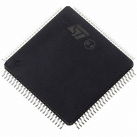
ST10F276Z5T3 STMicroelectronics, ST10F276Z5T3 Datasheet - Page 206

ST10F276Z5T3
Manufacturer Part Number
ST10F276Z5T3
Description
MCU 16BIT 832KBIT FLASH 144-TQFP
Manufacturer
STMicroelectronics
Series
ST10r
Datasheet
1.ST10F276Z5T3.pdf
(239 pages)
Specifications of ST10F276Z5T3
Core Processor
ST10
Core Size
16-Bit
Speed
40MHz
Connectivity
ASC, CAN, EBI/EMI, I²C, SSC, UART/USART
Peripherals
POR, PWM, WDT
Number Of I /o
111
Program Memory Size
832KB (832K x 8)
Program Memory Type
FLASH
Ram Size
68K x 8
Voltage - Supply (vcc/vdd)
4.5 V ~ 5.5 V
Data Converters
A/D 24x10b
Oscillator Type
Internal
Operating Temperature
-40°C ~ 125°C
Package / Case
144-TQFP, 144-VQFP
Cpu Family
ST10
Device Core Size
16b
Frequency (max)
40MHz
Interface Type
CAN/I2C
Total Internal Ram Size
68KB
# I/os (max)
111
Number Of Timers - General Purpose
5
Operating Supply Voltage (typ)
5V
Operating Supply Voltage (max)
5.5V
Operating Supply Voltage (min)
4.5V
On-chip Adc
24-chx10-bit
Instruction Set Architecture
CISC/RISC
Operating Temp Range
-40C to 125C
Operating Temperature Classification
Automotive
Mounting
Surface Mount
Pin Count
144
Package Type
LQFP
Processor Series
ST10F27x
Core
ST10
Data Bus Width
16 bit
Data Ram Size
68 KB
Maximum Clock Frequency
40 MHz
Number Of Programmable I/os
111
Number Of Timers
5
Maximum Operating Temperature
+ 125 C
Mounting Style
SMD/SMT
Minimum Operating Temperature
- 40 C
For Use With
497-6399 - KIT DEV STARTER ST10F276Z5
Lead Free Status / RoHS Status
Lead free / RoHS Compliant
Eeprom Size
-
Lead Free Status / Rohs Status
Compliant
Available stocks
Company
Part Number
Manufacturer
Quantity
Price
Company:
Part Number:
ST10F276Z5T3
Manufacturer:
STMicroelectronics
Quantity:
10 000
Electrical characteristics
Note:
23.8.16
206/239
Table 104. External clock drive timing
1. The minimum value for the XTAL1 signal period is considered as the theoretical minimum. The real
2. 4-12 MHz is the input frequency range when using an external clock source. 64 MHz can be applied with
3. The input clock signal must reach the defined levels V
Figure 56. External clock drive XTAL1
When Direct Drive is selected, an external clock source can be used to drive XTAL1. The
maximum frequency of the external clock source depends on the duty cycle: When 64 MHz
is used, 50% duty cycle is granted (low phase = high phase = 7.8 ns); when for instance
32 MHz is used, a 25% duty cycle can be accepted (minimum phase, high or low, again
equal to 7.8 ns).
Memory cycle variables
The tables below use three variables which are derived from the BUSCONx registers and
represent the special characteristics of the programmed memory cycle. The following table
describes how these variables are computed.
Table 105. Memory cycle variables
t
t
t
t
t
t
t
t
Symbol
OSC
1
2
3
4
A
C
F
minimum value depends on the duty cycle of the input clock signal.
an external clock source only when Direct Drive mode is selected: In this case, the oscillator amplifier is
bypassed so it does not limit the input frequency.
SR
SR
SR
SR
Symbol
SR
XTAL1 period
High time
Low time
Rise time
Fall time
Parameter
ALE extension
Memory cycle time wait states
Memory tri-state time
(3)
(3)
(3)
(3)
(1) (2)
t
1
Description
15.625
Min.
Direct drive
f
6
–
CPU
V
= f
IH2
XTAL
Max.
–
–
2
t
2
t
3
IL2
Direct drive with
and V
f
Min.
83.3
CPU
3
–
prescaler
t
V
OSC
IH2
IL2
= f
TCL x [ALECTL]
2TCL x (15 - [MCTC])
2TCL x (1 - [MTTC])
.
XTAL
Max.
250
–
2
/ 2
f
Min.
83.3
CPU
Values
6
–
PLL usage
= f
t
4
XTAL
Max.
ST10F276Z5
250
–
2
x F
Unit
ns


