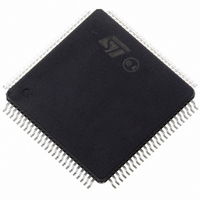
ST10F276Z5T3 STMicroelectronics, ST10F276Z5T3 Datasheet - Page 175

ST10F276Z5T3
Manufacturer Part Number
ST10F276Z5T3
Description
MCU 16BIT 832KBIT FLASH 144-TQFP
Manufacturer
STMicroelectronics
Series
ST10r
Datasheet
1.ST10F276Z5T3.pdf
(239 pages)
Specifications of ST10F276Z5T3
Core Processor
ST10
Core Size
16-Bit
Speed
40MHz
Connectivity
ASC, CAN, EBI/EMI, I²C, SSC, UART/USART
Peripherals
POR, PWM, WDT
Number Of I /o
111
Program Memory Size
832KB (832K x 8)
Program Memory Type
FLASH
Ram Size
68K x 8
Voltage - Supply (vcc/vdd)
4.5 V ~ 5.5 V
Data Converters
A/D 24x10b
Oscillator Type
Internal
Operating Temperature
-40°C ~ 125°C
Package / Case
144-TQFP, 144-VQFP
Cpu Family
ST10
Device Core Size
16b
Frequency (max)
40MHz
Interface Type
CAN/I2C
Total Internal Ram Size
68KB
# I/os (max)
111
Number Of Timers - General Purpose
5
Operating Supply Voltage (typ)
5V
Operating Supply Voltage (max)
5.5V
Operating Supply Voltage (min)
4.5V
On-chip Adc
24-chx10-bit
Instruction Set Architecture
CISC/RISC
Operating Temp Range
-40C to 125C
Operating Temperature Classification
Automotive
Mounting
Surface Mount
Pin Count
144
Package Type
LQFP
Processor Series
ST10F27x
Core
ST10
Data Bus Width
16 bit
Data Ram Size
68 KB
Maximum Clock Frequency
40 MHz
Number Of Programmable I/os
111
Number Of Timers
5
Maximum Operating Temperature
+ 125 C
Mounting Style
SMD/SMT
Minimum Operating Temperature
- 40 C
For Use With
497-6399 - KIT DEV STARTER ST10F276Z5
Lead Free Status / RoHS Status
Lead free / RoHS Compliant
Eeprom Size
-
Lead Free Status / Rohs Status
Compliant
Available stocks
Company
Part Number
Manufacturer
Quantity
Price
Company:
Part Number:
ST10F276Z5T3
Manufacturer:
STMicroelectronics
Quantity:
10 000
ST10F276Z5
Table 86.
When CAN1, CAN2, RTC, XASC, XSSC, I
all disabled via XPERCON setting, then any access in the address range 00’E800h -
00’EFFFh is directed to external memory interface, using the BUSCONx register
corresponding to the address matching ADDRSELx register. All pins used for X-Peripherals
can be used as General Purpose I/O whenever the related module is not enabled.
XRTCEN
XPWMEN
XFLASHEN
XASCEN
XSSCEN
XI2CEN
XMISCEN
Bit
ESFR description (continued)
RTC enable
‘0’: Accesses to the on-chip RTC module are disabled, external access performed.
Address range 00’ED00h-00’EDFF is directed to external memory only if
CAN1EN, CAN2EN, XASCEN, XSSCEN, XI2CEN, XPWMEN and XMISCEN are
‘0’ also.
‘1’: The on-chip RTC module is enabled and can be accessed.
XPWM enable
‘0’: Accesses to the on-chip XPWM module are disabled, external access
performed. Address range 00’EC00h-00’ECFF is directed to external memory only
if CAN1EN, CAN2EN, XASCEN, XSSCEN, XI2CEN, XRTCEN and XMISCEN are
‘0’ also.
‘1’: The on-chip XPWM module is enabled and can be accessed.
XFlash enable bit
‘0’: Accesses to the on-chip XFlash and Flash registers are disabled, external
access performed. Address range 09’0000h-0E’FFFFh is directed to external
memory only if XRAM2EN is ‘0’ also.
‘1’: The on-chip XFlash is enabled and can be accessed.
XASC enable bit
‘0’: Accesses to the on-chip XASC are disabled, external access performed.
Address range 00’E900h-00’E9FFh is directed to external memory only if
CAN1EN, CAN2EN, XRTCEN, XASCEN, XI2CEN, XPWMEN and XMISCEN are
‘0’ also.
‘1’: The on-chip XASC is enabled and can be accessed.
XSSC enable bit
‘0’: Accesses to the on-chip XSSC are disabled, external access performed.
Address range 00’E800h-00’E8FFh is directed to external memory only if
CAN1EN, CAN2EN, XRTCEN, XASCEN, XI2CEN, XPWMEN and XMISCEN are
‘0’ also.
‘1’: The on-chip XSSC is enabled and can be accessed.
I
‘0’: Accesses to the on-chip I
range 00’EA00h-00’EAFFh is directed to external memory only if CAN1EN,
CAN2EN, XRTCEN, XASCEN, XSSCEN, XPWMEN and XMISCEN are ‘0’ also.
‘1’: The on-chip I
XBUS additional features enable bit
‘0’: Accesses to the Additional Miscellaneous Features is disabled. Address range
00’EB00h-00’EBFFh is directed to external memory only if CAN1EN, CAN2EN,
XRTCEN, XASCEN, XSSCEN, XPWMEN and XI2CEN are ‘0’ also.
‘1’: The Additional Features are enabled and can be accessed.
2
C enable bit
2
C is enabled and can be accessed.
2
2
C, XPWM and the XBUS Additional Features are
C are disabled, external access performed. Address
Function
Register set
175/239


