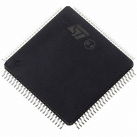
ST10F276Z5T3 STMicroelectronics, ST10F276Z5T3 Datasheet - Page 45

ST10F276Z5T3
Manufacturer Part Number
ST10F276Z5T3
Description
MCU 16BIT 832KBIT FLASH 144-TQFP
Manufacturer
STMicroelectronics
Series
ST10r
Datasheet
1.ST10F276Z5T3.pdf
(239 pages)
Specifications of ST10F276Z5T3
Core Processor
ST10
Core Size
16-Bit
Speed
40MHz
Connectivity
ASC, CAN, EBI/EMI, I²C, SSC, UART/USART
Peripherals
POR, PWM, WDT
Number Of I /o
111
Program Memory Size
832KB (832K x 8)
Program Memory Type
FLASH
Ram Size
68K x 8
Voltage - Supply (vcc/vdd)
4.5 V ~ 5.5 V
Data Converters
A/D 24x10b
Oscillator Type
Internal
Operating Temperature
-40°C ~ 125°C
Package / Case
144-TQFP, 144-VQFP
Cpu Family
ST10
Device Core Size
16b
Frequency (max)
40MHz
Interface Type
CAN/I2C
Total Internal Ram Size
68KB
# I/os (max)
111
Number Of Timers - General Purpose
5
Operating Supply Voltage (typ)
5V
Operating Supply Voltage (max)
5.5V
Operating Supply Voltage (min)
4.5V
On-chip Adc
24-chx10-bit
Instruction Set Architecture
CISC/RISC
Operating Temp Range
-40C to 125C
Operating Temperature Classification
Automotive
Mounting
Surface Mount
Pin Count
144
Package Type
LQFP
Processor Series
ST10F27x
Core
ST10
Data Bus Width
16 bit
Data Ram Size
68 KB
Maximum Clock Frequency
40 MHz
Number Of Programmable I/os
111
Number Of Timers
5
Maximum Operating Temperature
+ 125 C
Mounting Style
SMD/SMT
Minimum Operating Temperature
- 40 C
For Use With
497-6399 - KIT DEV STARTER ST10F276Z5
Lead Free Status / RoHS Status
Lead free / RoHS Compliant
Eeprom Size
-
Lead Free Status / Rohs Status
Compliant
Available stocks
Company
Part Number
Manufacturer
Quantity
Price
Company:
Part Number:
ST10F276Z5T3
Manufacturer:
STMicroelectronics
Quantity:
10 000
ST10F276Z5
4.7
Example 2: Enable Access and Debug Protection.
Example 3: Disable in a permanent way Access and Debug Protection.
Example 4: Enable again in a permanent way Access and Debug Protection, after having
disabled them.
Disable and re-enable of Access and Debug Protection in a permanent way (as shown by
examples 3 and 4) can be done for a maximum of 16 times.
Write operation summary
In general, each write operation is started through a sequence of 3 steps:
1.
2.
3.
Once selected, but not yet started, one operation can be canceled by resetting the operation
selection bit.
A summary of the available Flash Module Write Operations are shown in the following
Table
FCR0H|= 0x0100;/*Set SPR in FCR0H*/
FARL = 0xDFB8;/*Load Add of register FNVAPR0 in FARL*/
FARH = 0x000E;/*Load Add of register FNVAPR0 in FARH*/
FDR0L = 0xFFFC;/*Load Data in FDR0L*/
FCR0H|= 0x8000;/*Operation start*/
FCR0H|= 0x0100;/*Set SPR in FCR0H*/
FARL = 0xDFBC;/*Load Add of register FNVAPR1L in FARL*/
FARH = 0x000E;/*Load Add of register FNVAPR1L in FARH*/
FDR0L = 0xFFFE; /*Load Data in FDR0L for clearing PDS0*/
FCR0H|= 0x8000;/*Operation start*/
FCR0H|= 0x0100;/*Set SPR in FCR0H*/
FARL = 0xDFBC;/*Load Add register FNVAPR1H in FARL*/
FARH
FDR0H = 0xFFFE;/*Load Data in FDR0H for clearing PEN0*/
FCR0H|= 0x8000;/*Operation start*/
The first instruction is used to select the desired operation by setting its corresponding
selection bit in the Flash Control Register 0. This instruction is also used to select in
which Flash Module to apply the Write Operation (by setting/resetting bit SMOD).
The second step is the definition of the Address and Data for programming or the
Sectors or Banks to erase.
The last instruction is used to start the write operation, by setting the start bit WMS in
the FCR0.
28.
= 0x000E;/*Load Add register FNVAPR1H in FARH*/
Internal Flash memory
45/239


