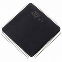
ST10F276Z5T3 STMicroelectronics, ST10F276Z5T3 Datasheet - Page 15

ST10F276Z5T3
Manufacturer Part Number
ST10F276Z5T3
Description
MCU 16BIT 832KBIT FLASH 144-TQFP
Manufacturer
STMicroelectronics
Series
ST10r
Datasheet
1.ST10F276Z5T3.pdf
(239 pages)
Specifications of ST10F276Z5T3
Core Processor
ST10
Core Size
16-Bit
Speed
40MHz
Connectivity
ASC, CAN, EBI/EMI, I²C, SSC, UART/USART
Peripherals
POR, PWM, WDT
Number Of I /o
111
Program Memory Size
832KB (832K x 8)
Program Memory Type
FLASH
Ram Size
68K x 8
Voltage - Supply (vcc/vdd)
4.5 V ~ 5.5 V
Data Converters
A/D 24x10b
Oscillator Type
Internal
Operating Temperature
-40°C ~ 125°C
Package / Case
144-TQFP, 144-VQFP
Cpu Family
ST10
Device Core Size
16b
Frequency (max)
40MHz
Interface Type
CAN/I2C
Total Internal Ram Size
68KB
# I/os (max)
111
Number Of Timers - General Purpose
5
Operating Supply Voltage (typ)
5V
Operating Supply Voltage (max)
5.5V
Operating Supply Voltage (min)
4.5V
On-chip Adc
24-chx10-bit
Instruction Set Architecture
CISC/RISC
Operating Temp Range
-40C to 125C
Operating Temperature Classification
Automotive
Mounting
Surface Mount
Pin Count
144
Package Type
LQFP
Processor Series
ST10F27x
Core
ST10
Data Bus Width
16 bit
Data Ram Size
68 KB
Maximum Clock Frequency
40 MHz
Number Of Programmable I/os
111
Number Of Timers
5
Maximum Operating Temperature
+ 125 C
Mounting Style
SMD/SMT
Minimum Operating Temperature
- 40 C
For Use With
497-6399 - KIT DEV STARTER ST10F276Z5
Lead Free Status / RoHS Status
Lead free / RoHS Compliant
Eeprom Size
-
Lead Free Status / Rohs Status
Compliant
Available stocks
Company
Part Number
Manufacturer
Quantity
Price
Company:
Part Number:
ST10F276Z5T3
Manufacturer:
STMicroelectronics
Quantity:
10 000
ST10F276Z5
●
●
●
●
●
●
●
●
●
●
●
●
●
●
restrictions and functional differences due to the XBUS peculiarities are present
between the classic PWM, and the new XPWM.
An I
CLKOUT function can output either the CPU clock (like in ST10F269) or a software
programmable prescaled value of the CPU clock.
Embedded memory size has been significantly increased (both Flash and RAM).
PLL multiplication factors have been adapted to new frequency range.
A/D Converter is not fully compatible versus ST10F269 (timing and programming
model). Formula for the conversion time is still valid, while the sampling phase
programming model is different.
Besides, additional 8 channels are available on P1L pins as alternate function: the
accuracy reachable with these extra channels is reduced with respect to the standard
Port5 channels.
External Memory bus potential limitations on maximum speed and maximum
capacitance load could be introduced (under evaluation): ST10F276Z5 will probably
not be able to address an external memory at 64 MHz with 0 wait states (under
evaluation).
XPERCON register bit mapping modified according to new peripherals implementation
(not fully compatible with ST10F269).
Bond-out chip for emulation (ST10R201) cannot achieve more than 50 MHz at room
temperature (so no real-time emulation possible at maximum speed).
Input section characteristics are different. The threshold programmability is extended to
all port pins (additional XPICON register); it is possible to select standard TTL (with up
to 500 mV of hysteresis) and standard CMOS (with up to 800 mV of hysteresis).
Output transition is not programmable.
CAN module is enhanced: the ST10F276Z5 implements two C-CAN modules, so the
programming model is slightly different. Besides, the possibility to map in parallel the
two CAN modules is added (on P4.5/P4.6).
On-chip main oscillator input frequency range has been reshaped, reducing it from 1-
25 MHz down to 4-12 MHz. This is a high performance oscillator amplifier, providing a
very high negative resistance and wide oscillation amplitude: when this on-chip
amplifier is used as reference for real-time clock module, the power-down consumption
is dominated by the consumption of the oscillator amplifier itself. A metal option is
added to offer a low power oscillator amplifier working in the range of 4-8 MHz: this will
allow a power consumption reduction when real-time clock is running in Power-down
mode using as reference the on-chip main oscillator clock.
A second on-chip oscillator amplifier circuit (32 kHz) is implemented for low power
modes: it can be used to provide the reference to the real-time clock counter (either in
Power-down or Standby mode). Pin XTAL3 and XTAL4 replace a couple of V
pins of ST10F269.
Possibility to re-program internal XBUS chip select window characteristics (XRAM2 and
XFLASH address window) is added.
2
C interface on the XBUS is added (see X-I
2
C or simply I
2
C interface).
Description
DD
/V
15/239
SS


