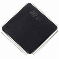
ST10F276Z5T3 STMicroelectronics, ST10F276Z5T3 Datasheet - Page 52

ST10F276Z5T3
Manufacturer Part Number
ST10F276Z5T3
Description
MCU 16BIT 832KBIT FLASH 144-TQFP
Manufacturer
STMicroelectronics
Series
ST10r
Datasheet
1.ST10F276Z5T3.pdf
(239 pages)
Specifications of ST10F276Z5T3
Core Processor
ST10
Core Size
16-Bit
Speed
40MHz
Connectivity
ASC, CAN, EBI/EMI, I²C, SSC, UART/USART
Peripherals
POR, PWM, WDT
Number Of I /o
111
Program Memory Size
832KB (832K x 8)
Program Memory Type
FLASH
Ram Size
68K x 8
Voltage - Supply (vcc/vdd)
4.5 V ~ 5.5 V
Data Converters
A/D 24x10b
Oscillator Type
Internal
Operating Temperature
-40°C ~ 125°C
Package / Case
144-TQFP, 144-VQFP
Cpu Family
ST10
Device Core Size
16b
Frequency (max)
40MHz
Interface Type
CAN/I2C
Total Internal Ram Size
68KB
# I/os (max)
111
Number Of Timers - General Purpose
5
Operating Supply Voltage (typ)
5V
Operating Supply Voltage (max)
5.5V
Operating Supply Voltage (min)
4.5V
On-chip Adc
24-chx10-bit
Instruction Set Architecture
CISC/RISC
Operating Temp Range
-40C to 125C
Operating Temperature Classification
Automotive
Mounting
Surface Mount
Pin Count
144
Package Type
LQFP
Processor Series
ST10F27x
Core
ST10
Data Bus Width
16 bit
Data Ram Size
68 KB
Maximum Clock Frequency
40 MHz
Number Of Programmable I/os
111
Number Of Timers
5
Maximum Operating Temperature
+ 125 C
Mounting Style
SMD/SMT
Minimum Operating Temperature
- 40 C
For Use With
497-6399 - KIT DEV STARTER ST10F276Z5
Lead Free Status / RoHS Status
Lead free / RoHS Compliant
Eeprom Size
-
Lead Free Status / Rohs Status
Compliant
Available stocks
Company
Part Number
Manufacturer
Quantity
Price
Company:
Part Number:
ST10F276Z5T3
Manufacturer:
STMicroelectronics
Quantity:
10 000
- Current page: 52 of 239
- Download datasheet (3Mb)
Bootstrap loader
5.2.5
52/239
Figure 7.
Memory configuration in bootstrap loader mode
The configuration (that is, the accessibility) of the device memory areas after reset in
Bootstrap Loader mode differs from the standard case. Pin EA is evaluated when BSL mode
is selected to enable or to not enable the external bus:
●
●
Moreover, while in BSL mode, accesses to the internal IFLASH area are partially redirected:
●
●
●
●
●
Example
In default configuration, to program address 0, the user must put the value 01'0000h in the
FARL and FARH registers but to verify the content of the address 0 a read to 00'0000h must
be performed.
If EA = 1, the external bus is disabled (BUSACT0 = 0 in BUSCON0 register);
If EA = 0, the external bus is enabled (BUSACT0 = 1 in BUSCON0 register).
All code accesses are made from the special Test-Flash seen in the range 00’0000h to
00’01FFFh;
User IFLASH is only available for read and write accesses (Test-Flash cannot be read
or written);
Write accesses must be made with addresses starting in segment 1 from 01'0000h,
regardless of the value of ROMS1 bit in SYSCON register;
Read accesses are made in segment 0 or in segment 1 depending on the ROMS1
value;
In BSL mode, by default, ROMS1 = 0, so the first 32 Kbytes of IFlash are mapped in
segment 0.
P0L.4
Hardware provisions to activate the BSL
R
8kΩ max.
Circuit 1
P0L.4
P0L.4
External
signal
Normal boot
BSL
R
8kΩ max.
Circuit 2
P0L.4
ST10F276Z5
Related parts for ST10F276Z5T3
Image
Part Number
Description
Manufacturer
Datasheet
Request
R

Part Number:
Description:
MCU 16BIT 832K FLASH 144-LQFP
Manufacturer:
STMicroelectronics
Datasheet:

Part Number:
Description:
MCU 16BIT 832K FLASH 144-LQFP
Manufacturer:
STMicroelectronics
Datasheet:

Part Number:
Description:
MCU 16BIT 832K FLASH 144-PQFP
Manufacturer:
STMicroelectronics
Datasheet:

Part Number:
Description:
MCU 16BIT 832K FLASH 144-PQFP
Manufacturer:
STMicroelectronics
Datasheet:

Part Number:
Description:
16-bit Microcontrollers - MCU 16-Bit MCU 832 kByte 68 KB RAM CMOS
Manufacturer:
STMicroelectronics

Part Number:
Description:
STMicroelectronics [RIPPLE-CARRY BINARY COUNTER/DIVIDERS]
Manufacturer:
STMicroelectronics
Datasheet:

Part Number:
Description:
STMicroelectronics [LIQUID-CRYSTAL DISPLAY DRIVERS]
Manufacturer:
STMicroelectronics
Datasheet:

Part Number:
Description:
BOARD EVAL FOR MEMS SENSORS
Manufacturer:
STMicroelectronics
Datasheet:

Part Number:
Description:
NPN TRANSISTOR POWER MODULE
Manufacturer:
STMicroelectronics
Datasheet:

Part Number:
Description:
TURBOSWITCH ULTRA-FAST HIGH VOLTAGE DIODE
Manufacturer:
STMicroelectronics
Datasheet:

Part Number:
Description:
Manufacturer:
STMicroelectronics
Datasheet:

Part Number:
Description:
DIODE / SCR MODULE
Manufacturer:
STMicroelectronics
Datasheet:


