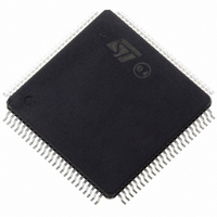
ST10F276Z5T3 STMicroelectronics, ST10F276Z5T3 Datasheet - Page 29

ST10F276Z5T3
Manufacturer Part Number
ST10F276Z5T3
Description
MCU 16BIT 832KBIT FLASH 144-TQFP
Manufacturer
STMicroelectronics
Series
ST10r
Datasheet
1.ST10F276Z5T3.pdf
(239 pages)
Specifications of ST10F276Z5T3
Core Processor
ST10
Core Size
16-Bit
Speed
40MHz
Connectivity
ASC, CAN, EBI/EMI, I²C, SSC, UART/USART
Peripherals
POR, PWM, WDT
Number Of I /o
111
Program Memory Size
832KB (832K x 8)
Program Memory Type
FLASH
Ram Size
68K x 8
Voltage - Supply (vcc/vdd)
4.5 V ~ 5.5 V
Data Converters
A/D 24x10b
Oscillator Type
Internal
Operating Temperature
-40°C ~ 125°C
Package / Case
144-TQFP, 144-VQFP
Cpu Family
ST10
Device Core Size
16b
Frequency (max)
40MHz
Interface Type
CAN/I2C
Total Internal Ram Size
68KB
# I/os (max)
111
Number Of Timers - General Purpose
5
Operating Supply Voltage (typ)
5V
Operating Supply Voltage (max)
5.5V
Operating Supply Voltage (min)
4.5V
On-chip Adc
24-chx10-bit
Instruction Set Architecture
CISC/RISC
Operating Temp Range
-40C to 125C
Operating Temperature Classification
Automotive
Mounting
Surface Mount
Pin Count
144
Package Type
LQFP
Processor Series
ST10F27x
Core
ST10
Data Bus Width
16 bit
Data Ram Size
68 KB
Maximum Clock Frequency
40 MHz
Number Of Programmable I/os
111
Number Of Timers
5
Maximum Operating Temperature
+ 125 C
Mounting Style
SMD/SMT
Minimum Operating Temperature
- 40 C
For Use With
497-6399 - KIT DEV STARTER ST10F276Z5
Lead Free Status / RoHS Status
Lead free / RoHS Compliant
Eeprom Size
-
Lead Free Status / Rohs Status
Compliant
Available stocks
Company
Part Number
Manufacturer
Quantity
Price
Company:
Part Number:
ST10F276Z5T3
Manufacturer:
STMicroelectronics
Quantity:
10 000
ST10F276Z5
Note:
4.3.1
4.4
4.4.1
Bank, or from the other module or again from another memory (internal RAM or external
memory).
During a Write operation, when bit LOCK of FCR0 is set, it is forbidden to write into the
Flash Control Registers.
Power supply drop
If during a write operation the internal low voltage supply drops below a certain internal
voltage threshold, any write operation running is suddenly interrupted and the modules are
reset to Read mode. At following Power-on, an interrupted Flash write operation must be
repeated.
Registers description
Flash control register 0 low
The Flash control register 0 low (FCR0L) together with the Flash control register 0 high
(FCR0H) is used to enable and to monitor all the write operations for both the Flash
modules. The user has no access in write mode to the test-Flash (B0TF). Besides, test-
Flash block is seen by the user in Bootstrap mode only.
FCR0L (0x0E 0000)
Table 7.
BSY(3:2)
15
Bit
14
Flash control register 0 low
13
Bank 3:2 Busy (XFLASH)
These bits indicate that a write operation is running on the corresponding Bank of
XFLASH. They are automatically set when bit WMS is set. Setting Protection
operation sets bit BSY2 (since protection registers are in the Block B2). When these
bits are set every read access to the corresponding Bank will output invalid data
(software trap 009Bh), while every write access to the Bank will be ignored. At the end
of the write operation or during a Program or Erase Suspend these bits are
automatically reset and the Bank returns to read mode. After a Program or Erase
Resume these bits are automatically set again.
12
reserved
11
10
9
FCR
8
7
Function
BSY1 BSY0 LOCK res. BSY3 BSY2 res.
R
6
R
5
R
4
Internal Flash memory
3
Reset value: 0000h
R
2
R
1
29/239
0


