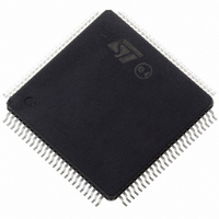
ST10F276Z5T3 STMicroelectronics, ST10F276Z5T3 Datasheet - Page 232

ST10F276Z5T3
Manufacturer Part Number
ST10F276Z5T3
Description
MCU 16BIT 832KBIT FLASH 144-TQFP
Manufacturer
STMicroelectronics
Series
ST10r
Datasheet
1.ST10F276Z5T3.pdf
(239 pages)
Specifications of ST10F276Z5T3
Core Processor
ST10
Core Size
16-Bit
Speed
40MHz
Connectivity
ASC, CAN, EBI/EMI, I²C, SSC, UART/USART
Peripherals
POR, PWM, WDT
Number Of I /o
111
Program Memory Size
832KB (832K x 8)
Program Memory Type
FLASH
Ram Size
68K x 8
Voltage - Supply (vcc/vdd)
4.5 V ~ 5.5 V
Data Converters
A/D 24x10b
Oscillator Type
Internal
Operating Temperature
-40°C ~ 125°C
Package / Case
144-TQFP, 144-VQFP
Cpu Family
ST10
Device Core Size
16b
Frequency (max)
40MHz
Interface Type
CAN/I2C
Total Internal Ram Size
68KB
# I/os (max)
111
Number Of Timers - General Purpose
5
Operating Supply Voltage (typ)
5V
Operating Supply Voltage (max)
5.5V
Operating Supply Voltage (min)
4.5V
On-chip Adc
24-chx10-bit
Instruction Set Architecture
CISC/RISC
Operating Temp Range
-40C to 125C
Operating Temperature Classification
Automotive
Mounting
Surface Mount
Pin Count
144
Package Type
LQFP
Processor Series
ST10F27x
Core
ST10
Data Bus Width
16 bit
Data Ram Size
68 KB
Maximum Clock Frequency
40 MHz
Number Of Programmable I/os
111
Number Of Timers
5
Maximum Operating Temperature
+ 125 C
Mounting Style
SMD/SMT
Minimum Operating Temperature
- 40 C
For Use With
497-6399 - KIT DEV STARTER ST10F276Z5
Lead Free Status / RoHS Status
Lead free / RoHS Compliant
Eeprom Size
-
Lead Free Status / Rohs Status
Compliant
Available stocks
Company
Part Number
Manufacturer
Quantity
Price
Company:
Part Number:
ST10F276Z5T3
Manufacturer:
STMicroelectronics
Quantity:
10 000
- Current page: 232 of 239
- Download datasheet (3Mb)
Known limitations
24.1.4
24.1.5
232/239
Spurious BREQ pulse in slave mode during external bus arbitration
phase
Description
Sporadic bus errors may occur when the device operates as a slave and the HOLD signal is
used for external bus arbitration.
After the slave has been granted the bus, it deactivates sporadically BREQ signal for a short
time, even though its access to the bus has not been completed. The master then starts
accessing the bus, thus causing a bus conflict between master and slave.
Workaround
To avoid producing any spurious BREQ pulse during slave external bus arbitrations, it is
necessary to ensure that the time between the HLDA assertion (Bus Acknowledge from
Master device) and the following HOLD falling edge (Bus Request from Master) is longer
than three clock cycles.
This can be achieved by delaying the HOLD signal with an RC circuit (see
Figure 72. Connecting an ST10 in slave mode
Executing PWRDN instructions
Description
The Power-down mode is not entered and the PWRDN instruction is ignored in the following
cases:
●
●
The PWRDN instruction is executed while NMI is high (PWDCFG bit of the SYSCON
register cleared)
The PWRDN instruction is executed while at least one of the Port 2 pins used to exit
from Power-down mode (PWDCFG bit of the SYSCON register is set) is at the active
level.
Master
HOLD
HLDA
BREQ
V
SS
BREQ (P6.7)
HOLD (P6.5)
HLDA (P6.6)
ST10 in Slave mode
Figure
ST10F276Z5
72).
Related parts for ST10F276Z5T3
Image
Part Number
Description
Manufacturer
Datasheet
Request
R

Part Number:
Description:
MCU 16BIT 832K FLASH 144-LQFP
Manufacturer:
STMicroelectronics
Datasheet:

Part Number:
Description:
MCU 16BIT 832K FLASH 144-LQFP
Manufacturer:
STMicroelectronics
Datasheet:

Part Number:
Description:
MCU 16BIT 832K FLASH 144-PQFP
Manufacturer:
STMicroelectronics
Datasheet:

Part Number:
Description:
MCU 16BIT 832K FLASH 144-PQFP
Manufacturer:
STMicroelectronics
Datasheet:

Part Number:
Description:
16-bit Microcontrollers - MCU 16-Bit MCU 832 kByte 68 KB RAM CMOS
Manufacturer:
STMicroelectronics

Part Number:
Description:
STMicroelectronics [RIPPLE-CARRY BINARY COUNTER/DIVIDERS]
Manufacturer:
STMicroelectronics
Datasheet:

Part Number:
Description:
STMicroelectronics [LIQUID-CRYSTAL DISPLAY DRIVERS]
Manufacturer:
STMicroelectronics
Datasheet:

Part Number:
Description:
BOARD EVAL FOR MEMS SENSORS
Manufacturer:
STMicroelectronics
Datasheet:

Part Number:
Description:
NPN TRANSISTOR POWER MODULE
Manufacturer:
STMicroelectronics
Datasheet:

Part Number:
Description:
TURBOSWITCH ULTRA-FAST HIGH VOLTAGE DIODE
Manufacturer:
STMicroelectronics
Datasheet:

Part Number:
Description:
Manufacturer:
STMicroelectronics
Datasheet:

Part Number:
Description:
DIODE / SCR MODULE
Manufacturer:
STMicroelectronics
Datasheet:


