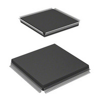
HD64F7051SFJ20V Renesas Electronics America, HD64F7051SFJ20V Datasheet - Page 162

HD64F7051SFJ20V
Manufacturer Part Number
HD64F7051SFJ20V
Description
MCU 5V 256K J-TEMP PB-FREE QFP-1
Manufacturer
Renesas Electronics America
Series
SuperH® SH7050r
Datasheet
1.HD64F7050SFJ20V.pdf
(843 pages)
Specifications of HD64F7051SFJ20V
Core Processor
SH-2
Core Size
32-Bit
Speed
20MHz
Connectivity
EBI/EMI, SCI
Peripherals
DMA, WDT
Number Of I /o
102
Program Memory Size
256KB (256K x 8)
Program Memory Type
FLASH
Ram Size
10K x 8
Voltage - Supply (vcc/vdd)
4.5 V ~ 5.5 V
Data Converters
A/D 16x10b
Oscillator Type
Internal
Operating Temperature
-40°C ~ 85°C
Package / Case
168-QFP
Lead Free Status / RoHS Status
Lead free / RoHS Compliant
Eeprom Size
-
Available stocks
Company
Part Number
Manufacturer
Quantity
Price
Company:
Part Number:
HD64F7051SFJ20V
Manufacturer:
RENESAS
Quantity:
101
Part Number:
HD64F7051SFJ20V
Manufacturer:
RENESAS/瑞萨
Quantity:
20 000
- Current page: 162 of 843
- Download datasheet (5Mb)
Section 9 Direct Memory Access Controller (DMAC)
Chan-
nel
3
Shared DMA operation
Notes: Registers are accessed in three cycles when using word access and six cycles when using
9.2
9.2.1
DMA source address registers 0–3 (SAR0–SAR3) are 32-bit read/write registers that specify the
source address of a DMA transfer. These registers have a count function, and during a DMA
transfer, they indicate the next source address. In single-address mode, SAR values are ignored
when a device with DACK has been specified as the transfer source.
Specify a 16-bit boundary when performing 16-bit data transfers, and a 32-bit boundary when
performing 32-bit data transfers. Operation cannot be guaranteed if any other addresses are set.
The initial value after power-on resets and in software standby mode is undefined.
Rev. 5.00 Jan 06, 2006 page 140 of 818
REJ09B0273-0500
longword access.
Do not attempt to access an empty address.
1. Write 0 after reading 1 in bit 1 of CHCR0–CHCR3 and in bits 1 and 2 of the DMAOR to
2. For 16-bit access of SAR0–SAR3, DAR0–DAR3, and CHCR0–CHCR3, the 16-bit value
3. DMATCR has a 24-bit configuration: bits 0–23. Writing to the upper 8 bits (bits 24–31)
4. Do not make 32-bit access for DMAOR.
Name
DMA source address
register 3
DMA destination
address register 3
DMA transfer count
register 3
DMA channel control
register 3
register
Register Descriptions
DMA Source Address Registers 0–3 (SAR0–SAR3)
clear flags. No other writes are allowed.
on the side not accessed is held.
is invalid, and these bits always read 0.
Abbrevi-
ation
SAR3
DAR3
DMATCR3 R/W
CHCR3
DMAOR
R/W
R/W
R/W
R/W *
R/W *
1
1
Initial
Value
Undefined
Undefined
Undefined
H'00000000 H'FFFF86FC 32 bit
H'0000
Address
H'FFFF86F0 32 bit
H'FFFF86F4 32 bit
H'FFFF86F8 32 bit
H'FFFF86B0 16 bit
Register
Size
Access
Size
16, 32 *
16, 32 *
32 *
16, 32 *
8, 16 *
3
4
2
2
2
Related parts for HD64F7051SFJ20V
Image
Part Number
Description
Manufacturer
Datasheet
Request
R

Part Number:
Description:
KIT STARTER FOR M16C/29
Manufacturer:
Renesas Electronics America
Datasheet:

Part Number:
Description:
KIT STARTER FOR R8C/2D
Manufacturer:
Renesas Electronics America
Datasheet:

Part Number:
Description:
R0K33062P STARTER KIT
Manufacturer:
Renesas Electronics America
Datasheet:

Part Number:
Description:
KIT STARTER FOR R8C/23 E8A
Manufacturer:
Renesas Electronics America
Datasheet:

Part Number:
Description:
KIT STARTER FOR R8C/25
Manufacturer:
Renesas Electronics America
Datasheet:

Part Number:
Description:
KIT STARTER H8S2456 SHARPE DSPLY
Manufacturer:
Renesas Electronics America
Datasheet:

Part Number:
Description:
KIT STARTER FOR R8C38C
Manufacturer:
Renesas Electronics America
Datasheet:

Part Number:
Description:
KIT STARTER FOR R8C35C
Manufacturer:
Renesas Electronics America
Datasheet:

Part Number:
Description:
KIT STARTER FOR R8CL3AC+LCD APPS
Manufacturer:
Renesas Electronics America
Datasheet:

Part Number:
Description:
KIT STARTER FOR RX610
Manufacturer:
Renesas Electronics America
Datasheet:

Part Number:
Description:
KIT STARTER FOR R32C/118
Manufacturer:
Renesas Electronics America
Datasheet:

Part Number:
Description:
KIT DEV RSK-R8C/26-29
Manufacturer:
Renesas Electronics America
Datasheet:

Part Number:
Description:
KIT STARTER FOR SH7124
Manufacturer:
Renesas Electronics America
Datasheet:

Part Number:
Description:
KIT STARTER FOR H8SX/1622
Manufacturer:
Renesas Electronics America
Datasheet:

Part Number:
Description:
KIT DEV FOR SH7203
Manufacturer:
Renesas Electronics America
Datasheet:


