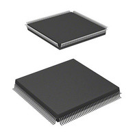
HD64F7051SFJ20V Renesas Electronics America, HD64F7051SFJ20V Datasheet - Page 556

HD64F7051SFJ20V
Manufacturer Part Number
HD64F7051SFJ20V
Description
MCU 5V 256K J-TEMP PB-FREE QFP-1
Manufacturer
Renesas Electronics America
Series
SuperH® SH7050r
Datasheet
1.HD64F7050SFJ20V.pdf
(843 pages)
Specifications of HD64F7051SFJ20V
Core Processor
SH-2
Core Size
32-Bit
Speed
20MHz
Connectivity
EBI/EMI, SCI
Peripherals
DMA, WDT
Number Of I /o
102
Program Memory Size
256KB (256K x 8)
Program Memory Type
FLASH
Ram Size
10K x 8
Voltage - Supply (vcc/vdd)
4.5 V ~ 5.5 V
Data Converters
A/D 16x10b
Oscillator Type
Internal
Operating Temperature
-40°C ~ 85°C
Package / Case
168-QFP
Lead Free Status / RoHS Status
Lead free / RoHS Compliant
Eeprom Size
-
Available stocks
Company
Part Number
Manufacturer
Quantity
Price
Company:
Part Number:
HD64F7051SFJ20V
Manufacturer:
RENESAS
Quantity:
101
Part Number:
HD64F7051SFJ20V
Manufacturer:
RENESAS/瑞萨
Quantity:
20 000
- Current page: 556 of 843
- Download datasheet (5Mb)
Section 17 I/O Ports (I/O)
17.9.2
The port H data register (PHDR) is a 16-bit read-only register that stores port H data. Bits
PH15DR to PH0DR correspond to pins PH15/AN15 to PH0/AN0.
Writes to these bits are ignored, and do not affect the pin states. When these bits are read, the pin
state, not the register value, is returned directly. However, 1 will be returned while A/D converter
analog input is being sampled. Table 17.16 summarizes port H data register read/write operations.
PHDR is not initialized by a power-on reset, or in hardware standby mode, software standby
mode, or sleep mode. (The bits always reflect the pin states.)
Table 17.16 Port H Data Register (PHDR) Read/Write Operations
Pin Input/Output
Input
n = 0 to 15
17.10
The output port drive buffers for the address bus pins (A20 to A0) and data bus pins (D15 to D0)
can be controlled by the POD (port output disable) pin input level. However, this function is
enabled only when the address bus pins (A20 to A0) and data bus pins (D15 to D0) are designated
as general output ports.
Output buffer control by means of POD is performed asynchronously from bus cycles.
POD
POD
0
1
Rev. 5.00 Jan 06, 2006 page 534 of 818
REJ09B0273-0500
POD
POD
Initial value:
R/W:
Bit:
Port H Data Register (PHDR)
POD (Port Output Disable)
PH15
DR
15
R
0
PH14
DR
14
Address Bus Pins (A20 to A0) and Data Bus Pins (D15 to D0)
(when Designated as Output Ports)
Enabled (high-impedance)
Disabled (general output)
R
0
Pin Function
General input
ANn
PH13
DR
13
R
0
PH12
DR
12
R
0
PH11
DR
11
R
0
PH10
DR
10
Read
Pin state is read
1 is read
R
0
PH9
DR
R
9
0
PH8
DR
R
8
0
PH7
DR
R
7
0
PH6
DR
R
6
0
Ignored (does not affect pin state)
Write
Ignored (does not affect pin state)
PH5
DR
R
5
0
PH4
DR
R
4
0
PH3
DR
R
3
0
PH2
DR
R
2
0
PH1
DR
R
1
0
PH0
DR
R
0
0
Related parts for HD64F7051SFJ20V
Image
Part Number
Description
Manufacturer
Datasheet
Request
R

Part Number:
Description:
KIT STARTER FOR M16C/29
Manufacturer:
Renesas Electronics America
Datasheet:

Part Number:
Description:
KIT STARTER FOR R8C/2D
Manufacturer:
Renesas Electronics America
Datasheet:

Part Number:
Description:
R0K33062P STARTER KIT
Manufacturer:
Renesas Electronics America
Datasheet:

Part Number:
Description:
KIT STARTER FOR R8C/23 E8A
Manufacturer:
Renesas Electronics America
Datasheet:

Part Number:
Description:
KIT STARTER FOR R8C/25
Manufacturer:
Renesas Electronics America
Datasheet:

Part Number:
Description:
KIT STARTER H8S2456 SHARPE DSPLY
Manufacturer:
Renesas Electronics America
Datasheet:

Part Number:
Description:
KIT STARTER FOR R8C38C
Manufacturer:
Renesas Electronics America
Datasheet:

Part Number:
Description:
KIT STARTER FOR R8C35C
Manufacturer:
Renesas Electronics America
Datasheet:

Part Number:
Description:
KIT STARTER FOR R8CL3AC+LCD APPS
Manufacturer:
Renesas Electronics America
Datasheet:

Part Number:
Description:
KIT STARTER FOR RX610
Manufacturer:
Renesas Electronics America
Datasheet:

Part Number:
Description:
KIT STARTER FOR R32C/118
Manufacturer:
Renesas Electronics America
Datasheet:

Part Number:
Description:
KIT DEV RSK-R8C/26-29
Manufacturer:
Renesas Electronics America
Datasheet:

Part Number:
Description:
KIT STARTER FOR SH7124
Manufacturer:
Renesas Electronics America
Datasheet:

Part Number:
Description:
KIT STARTER FOR H8SX/1622
Manufacturer:
Renesas Electronics America
Datasheet:

Part Number:
Description:
KIT DEV FOR SH7203
Manufacturer:
Renesas Electronics America
Datasheet:


