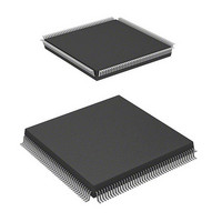
HD64F7051SFJ20V Renesas Electronics America, HD64F7051SFJ20V Datasheet - Page 470

HD64F7051SFJ20V
Manufacturer Part Number
HD64F7051SFJ20V
Description
MCU 5V 256K J-TEMP PB-FREE QFP-1
Manufacturer
Renesas Electronics America
Series
SuperH® SH7050r
Datasheet
1.HD64F7050SFJ20V.pdf
(843 pages)
Specifications of HD64F7051SFJ20V
Core Processor
SH-2
Core Size
32-Bit
Speed
20MHz
Connectivity
EBI/EMI, SCI
Peripherals
DMA, WDT
Number Of I /o
102
Program Memory Size
256KB (256K x 8)
Program Memory Type
FLASH
Ram Size
10K x 8
Voltage - Supply (vcc/vdd)
4.5 V ~ 5.5 V
Data Converters
A/D 16x10b
Oscillator Type
Internal
Operating Temperature
-40°C ~ 85°C
Package / Case
168-QFP
Lead Free Status / RoHS Status
Lead free / RoHS Compliant
Eeprom Size
-
Available stocks
Company
Part Number
Manufacturer
Quantity
Price
Company:
Part Number:
HD64F7051SFJ20V
Manufacturer:
RENESAS
Quantity:
101
Part Number:
HD64F7051SFJ20V
Manufacturer:
RENESAS/瑞萨
Quantity:
20 000
- Current page: 470 of 843
- Download datasheet (5Mb)
Section 14 A/D Converter
14.4
The A/D converter operates by successive approximations with 10-bit resolution. It has two
operating modes: single mode and scan mode. In single mode, conversion is performed once on
one specified channel, then ends. In scan mode, A/D conversion continues on one or more
specified channels until the ADST bit is cleared to 0.
14.4.1
Single mode, should be selected when only one A/D conversion on one channel is required. Single
mode is selected for A/D0 by setting the ADM1 and ADM0 bits in A/D control/status register 0
(ADSCR0) to 00, and for A/D1 by clearing the SCAN mode bit in ADCSR1 to 0. When the
ADST bit (in ADCR0 for A/D0, or in ADCSR1 for A/D1) is set to 1, A/D conversion is started in
single mode.
The ADST bit remains set to 1 during A/D conversion, and is automatically cleared to 0 when
conversion ends.
When conversion ends, the ADF flag in ADCSR is set to 1. If the ADIE bit in ADCSR is also 1,
an ADI interrupt is requested. To clear the ADF flag, first read ADF when set to 1, then write 0 in
ADF. If the DMAC is activated by the ADI interrupt, ADF is cleared automatically.
An example of the operation when analog input channel 1 (AN1) is selected and A/D conversion
is performed in single mode is described next. Figure 14.3 shows a timing diagram for this
example.
1. Single mode is selected (ADM1 = ADM0 = 0), input channel AN1 is selected (CH3 = CH2 =
2. When A/D conversion is completed, the result is transferred to ADDR1. At the same time the
3. Since ADF = 1 and ADIE = 1, an ADI interrupt is requested.
4. The A/D interrupt handling routine is started.
5. The routine reads ADF set to 1, then writes 0 in ADF.
6. The routine reads and processes the conversion result (ADDR1).
7. Execution of the A/D interrupt handling routine ends. After this, if the ADST bit is set to 1,
Rev. 5.00 Jan 06, 2006 page 448 of 818
REJ09B0273-0500
CH1 = 0, CH0 = 1), the A/D interrupt is enabled (ADIE = 1), and A/D conversion is started
(ADST = 1).
ADF flag is set to 1, the ADST bit is cleared to 0, and the A/D converter becomes idle.
A/D conversion starts again and steps 2 to 7 are repeated.
Operation
Single Mode
Related parts for HD64F7051SFJ20V
Image
Part Number
Description
Manufacturer
Datasheet
Request
R

Part Number:
Description:
KIT STARTER FOR M16C/29
Manufacturer:
Renesas Electronics America
Datasheet:

Part Number:
Description:
KIT STARTER FOR R8C/2D
Manufacturer:
Renesas Electronics America
Datasheet:

Part Number:
Description:
R0K33062P STARTER KIT
Manufacturer:
Renesas Electronics America
Datasheet:

Part Number:
Description:
KIT STARTER FOR R8C/23 E8A
Manufacturer:
Renesas Electronics America
Datasheet:

Part Number:
Description:
KIT STARTER FOR R8C/25
Manufacturer:
Renesas Electronics America
Datasheet:

Part Number:
Description:
KIT STARTER H8S2456 SHARPE DSPLY
Manufacturer:
Renesas Electronics America
Datasheet:

Part Number:
Description:
KIT STARTER FOR R8C38C
Manufacturer:
Renesas Electronics America
Datasheet:

Part Number:
Description:
KIT STARTER FOR R8C35C
Manufacturer:
Renesas Electronics America
Datasheet:

Part Number:
Description:
KIT STARTER FOR R8CL3AC+LCD APPS
Manufacturer:
Renesas Electronics America
Datasheet:

Part Number:
Description:
KIT STARTER FOR RX610
Manufacturer:
Renesas Electronics America
Datasheet:

Part Number:
Description:
KIT STARTER FOR R32C/118
Manufacturer:
Renesas Electronics America
Datasheet:

Part Number:
Description:
KIT DEV RSK-R8C/26-29
Manufacturer:
Renesas Electronics America
Datasheet:

Part Number:
Description:
KIT STARTER FOR SH7124
Manufacturer:
Renesas Electronics America
Datasheet:

Part Number:
Description:
KIT STARTER FOR H8SX/1622
Manufacturer:
Renesas Electronics America
Datasheet:

Part Number:
Description:
KIT DEV FOR SH7203
Manufacturer:
Renesas Electronics America
Datasheet:


