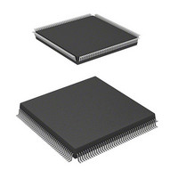
HD64F7051SFJ20V Renesas Electronics America, HD64F7051SFJ20V Datasheet - Page 532

HD64F7051SFJ20V
Manufacturer Part Number
HD64F7051SFJ20V
Description
MCU 5V 256K J-TEMP PB-FREE QFP-1
Manufacturer
Renesas Electronics America
Series
SuperH® SH7050r
Datasheet
1.HD64F7050SFJ20V.pdf
(843 pages)
Specifications of HD64F7051SFJ20V
Core Processor
SH-2
Core Size
32-Bit
Speed
20MHz
Connectivity
EBI/EMI, SCI
Peripherals
DMA, WDT
Number Of I /o
102
Program Memory Size
256KB (256K x 8)
Program Memory Type
FLASH
Ram Size
10K x 8
Voltage - Supply (vcc/vdd)
4.5 V ~ 5.5 V
Data Converters
A/D 16x10b
Oscillator Type
Internal
Operating Temperature
-40°C ~ 85°C
Package / Case
168-QFP
Lead Free Status / RoHS Status
Lead free / RoHS Compliant
Eeprom Size
-
Available stocks
Company
Part Number
Manufacturer
Quantity
Price
Company:
Part Number:
HD64F7051SFJ20V
Manufacturer:
RENESAS
Quantity:
101
Part Number:
HD64F7051SFJ20V
Manufacturer:
RENESAS/瑞萨
Quantity:
20 000
- Current page: 532 of 843
- Download datasheet (5Mb)
Section 16 Pin Function Controller (PFC)
16.3.13 Port G IO Register (PGIOR)
The port G IO register (PGIOR) is a 16-bit readable/writable register that selects the input/output
direction of the 16 pins in port G. Bits PG15IOR to PG0IOR correspond to pins
PG15/IRQ5/TIOB5 to PG0/ADTRG/IRQOUT. PGIOR is enabled when port G pins function as
general input/output pins (PG15 to PG0), serial clock pins (SCK1, SCK0), or timer input/output
pins (TIOD3, TIOA4, TIOB4, TIOC4, TIOD4, TIOA5, TIOB5), and is disabled otherwise.
When port G pins function as PG15 to PG0, SCK1 and SCK0, or TIOD3, TIOA4, TIOB4, TIOC4,
TIOD4, TIOA5, and TIOB5, a pin becomes an output when the corresponding bit in PGIOR is set
to 1, and an input when the bit is cleared to 0.
PGIOR is initialized to H'0000 by a power-on reset (excluding a WDT power-on reset), and in
hardware standby mode. It is not initialized in software standby mode or sleep mode.
16.3.14 Port G Control Registers 1 and 2 (PGCR1, PGCR2)
Port G control registers 1 and 2 (PGCR1, PGCR2) are 16-bit readable/writable registers that select
the functions of the 16 multiplex pins in port G. PGCR1 selects the functions of the pins for the
upper 8 bits in port G, and PGCR2 selects the functions of the pins for the lower 8 bits in port G.
PGCR1 and PGCR2 are initialized to H'0AAA and H'AA80, respectively, by a power-on reset
(excluding a WDT power-on reset), and in hardware standby mode. They are not initialized in
software standby mode or sleep mode.
Rev. 5.00 Jan 06, 2006 page 510 of 818
REJ09B0273-0500
Initial value:
R/W: R/W R/W R/W R/W R/W R/W R/W R/W R/W R/W R/W R/W R/W R/W R/W R/W
Bit:
PG1
IOR
15
0
5
PG1
IOR
14
0
4
PG1
IOR
13
0
3
PG1
IOR
12
0
2
PG1
IOR
11
0
1
PG1
IOR
10
0
0
PG9
IOR
9
0
PG8
IOR
8
0
PG7
IOR
7
0
PG6
IOR
6
0
PG5
IOR
5
0
PG4
IOR
4
0
PG3
IOR
3
0
PG2
IOR
2
0
PG1
IOR
1
0
PG0
IOR
0
0
Related parts for HD64F7051SFJ20V
Image
Part Number
Description
Manufacturer
Datasheet
Request
R

Part Number:
Description:
KIT STARTER FOR M16C/29
Manufacturer:
Renesas Electronics America
Datasheet:

Part Number:
Description:
KIT STARTER FOR R8C/2D
Manufacturer:
Renesas Electronics America
Datasheet:

Part Number:
Description:
R0K33062P STARTER KIT
Manufacturer:
Renesas Electronics America
Datasheet:

Part Number:
Description:
KIT STARTER FOR R8C/23 E8A
Manufacturer:
Renesas Electronics America
Datasheet:

Part Number:
Description:
KIT STARTER FOR R8C/25
Manufacturer:
Renesas Electronics America
Datasheet:

Part Number:
Description:
KIT STARTER H8S2456 SHARPE DSPLY
Manufacturer:
Renesas Electronics America
Datasheet:

Part Number:
Description:
KIT STARTER FOR R8C38C
Manufacturer:
Renesas Electronics America
Datasheet:

Part Number:
Description:
KIT STARTER FOR R8C35C
Manufacturer:
Renesas Electronics America
Datasheet:

Part Number:
Description:
KIT STARTER FOR R8CL3AC+LCD APPS
Manufacturer:
Renesas Electronics America
Datasheet:

Part Number:
Description:
KIT STARTER FOR RX610
Manufacturer:
Renesas Electronics America
Datasheet:

Part Number:
Description:
KIT STARTER FOR R32C/118
Manufacturer:
Renesas Electronics America
Datasheet:

Part Number:
Description:
KIT DEV RSK-R8C/26-29
Manufacturer:
Renesas Electronics America
Datasheet:

Part Number:
Description:
KIT STARTER FOR SH7124
Manufacturer:
Renesas Electronics America
Datasheet:

Part Number:
Description:
KIT STARTER FOR H8SX/1622
Manufacturer:
Renesas Electronics America
Datasheet:

Part Number:
Description:
KIT DEV FOR SH7203
Manufacturer:
Renesas Electronics America
Datasheet:


