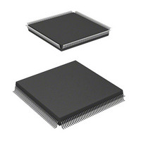
HD64F7051SFJ20V Renesas Electronics America, HD64F7051SFJ20V Datasheet - Page 580

HD64F7051SFJ20V
Manufacturer Part Number
HD64F7051SFJ20V
Description
MCU 5V 256K J-TEMP PB-FREE QFP-1
Manufacturer
Renesas Electronics America
Series
SuperH® SH7050r
Datasheet
1.HD64F7050SFJ20V.pdf
(843 pages)
Specifications of HD64F7051SFJ20V
Core Processor
SH-2
Core Size
32-Bit
Speed
20MHz
Connectivity
EBI/EMI, SCI
Peripherals
DMA, WDT
Number Of I /o
102
Program Memory Size
256KB (256K x 8)
Program Memory Type
FLASH
Ram Size
10K x 8
Voltage - Supply (vcc/vdd)
4.5 V ~ 5.5 V
Data Converters
A/D 16x10b
Oscillator Type
Internal
Operating Temperature
-40°C ~ 85°C
Package / Case
168-QFP
Lead Free Status / RoHS Status
Lead free / RoHS Compliant
Eeprom Size
-
Available stocks
Company
Part Number
Manufacturer
Quantity
Price
Company:
Part Number:
HD64F7051SFJ20V
Manufacturer:
RENESAS
Quantity:
101
Part Number:
HD64F7051SFJ20V
Manufacturer:
RENESAS/瑞萨
Quantity:
20 000
- Current page: 580 of 843
- Download datasheet (5Mb)
Section 18 ROM (128 kB Version)
Rev. 5.00 Jan 06, 2006 page 558 of 818
REJ09B0273-0500
Notes:
1. Transfer data in a byte unit. The lower eight bits of the start address to which data is written must be H'00, H'20, H'40, H'60, H'80, H'A0, H'C0, or
2. Read verify data in logword form (32 bits).
3. Even for bits to which data is already written, an additional write should be performed if their verify result is NG.
4. The write data storage area (32 bytes) and rewrite data storage area (32 bytes) must be located in RAM. The contents of the rewrite data storage
H'E0. Transfer 32-byte data even when writing fewer than 32 bytes. In this case, Set H'FF in unused addresses.
area are rewritten as writing progresses.
Rewrite data storage area
Write data storage area
Source data (D)
(32 byte)
(32 byte)
0
0
1
1
RAM
Increment address
Figure 18.7 Program/Program-Verify Flowchart
Verify data (V)
0
1
0
1
NG
Perform dummy-write of H'FF to verify address
Transfer rewrite data to rewrite data area
Successively write 32-byte data in rewrite data
Store 32 bytes write data in write
data area and rewrite data area
Rewrite data (X)
Clear SWE bit of FLMCR1
Clear PSU-bit of FLMCR1
Set SWE-bit of FLMCR1
area in RAM to flash memory
Clear PV-bit of FLMCR1
Set PSU-bit of FLMCR1
Write data= Verify data?
Clear P-bit of FLMCR1
Set PV-bit of FLMCR1
Set P-bit of FLMCR1
Operate rewrite data
Read verify data
verify complete?
Disable WDT
1
0
1
1
Enable WDT
32 byte data
Wait 500 s
Wait 10 s
Wait 50 s
Wait 10 s
Wait 10 s
Wait
Wait 2 s
Wait 4 s
Write end
m = 0
m = 0?
n = 1
Start
OK
OK
s
Rewrite should not be performed to bits already written to.
Write is incomplete; rewrite should be performed.
—
Left in the erased state.
OK
NG
NG
Description
*4
*1
Write start
Write end
*2
*3
*4
m = 1
Data writes must be performed in the memory-
erased state. Do not write additional data to an
address to which data is already written.
Clear SWE bit of FLMCR1
Write failure
n
400?
OK
NG
n
n + 1
Related parts for HD64F7051SFJ20V
Image
Part Number
Description
Manufacturer
Datasheet
Request
R

Part Number:
Description:
KIT STARTER FOR M16C/29
Manufacturer:
Renesas Electronics America
Datasheet:

Part Number:
Description:
KIT STARTER FOR R8C/2D
Manufacturer:
Renesas Electronics America
Datasheet:

Part Number:
Description:
R0K33062P STARTER KIT
Manufacturer:
Renesas Electronics America
Datasheet:

Part Number:
Description:
KIT STARTER FOR R8C/23 E8A
Manufacturer:
Renesas Electronics America
Datasheet:

Part Number:
Description:
KIT STARTER FOR R8C/25
Manufacturer:
Renesas Electronics America
Datasheet:

Part Number:
Description:
KIT STARTER H8S2456 SHARPE DSPLY
Manufacturer:
Renesas Electronics America
Datasheet:

Part Number:
Description:
KIT STARTER FOR R8C38C
Manufacturer:
Renesas Electronics America
Datasheet:

Part Number:
Description:
KIT STARTER FOR R8C35C
Manufacturer:
Renesas Electronics America
Datasheet:

Part Number:
Description:
KIT STARTER FOR R8CL3AC+LCD APPS
Manufacturer:
Renesas Electronics America
Datasheet:

Part Number:
Description:
KIT STARTER FOR RX610
Manufacturer:
Renesas Electronics America
Datasheet:

Part Number:
Description:
KIT STARTER FOR R32C/118
Manufacturer:
Renesas Electronics America
Datasheet:

Part Number:
Description:
KIT DEV RSK-R8C/26-29
Manufacturer:
Renesas Electronics America
Datasheet:

Part Number:
Description:
KIT STARTER FOR SH7124
Manufacturer:
Renesas Electronics America
Datasheet:

Part Number:
Description:
KIT STARTER FOR H8SX/1622
Manufacturer:
Renesas Electronics America
Datasheet:

Part Number:
Description:
KIT DEV FOR SH7203
Manufacturer:
Renesas Electronics America
Datasheet:


