Z16F2800100ZCOG Zilog, Z16F2800100ZCOG Datasheet - Page 196
Z16F2800100ZCOG
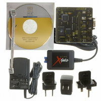
Manufacturer Part Number
Z16F2800100ZCOG
Description
DEV KIT FOR Z16F ZNEO
Manufacturer
Zilog
Series
ZNEO™r
Type
MCUr
Datasheets
1.Z16F2800100ZCOG.pdf
(2 pages)
2.Z16F2800100ZCOG.pdf
(30 pages)
3.Z16F2800100ZCOG.pdf
(388 pages)
Specifications of Z16F2800100ZCOG
Contents
Evaluation Board, Software and Documentation
For Use With/related Products
Z16F Series
For Use With
269-4661 - KIT ACC ETHERNET SMART CABLE
Lead Free Status / RoHS Status
Lead free / RoHS Compliant
Other names
269-4537


PS022008-0810
Throughput
ESPI Clock Phase and Polarity Control
ESPIEN1, 0 bits in the control register to
move the data, the transmit and receive data interrupts are disabled through the DIRQE bit
of the control register. In this case error interrupts still occurs and must be handled directly
by the software.
In MASTER mode the maximum SCK rate supported is one-half the system clock
frequency. This is achieved by programming the value 0001H into the baud rate high/low
register pair. Though each character is transferred at this rate, it is unlikely that software
interrupt routines or DMA keeps up with this rate. In SPI mode the transfer will
automatically pause between characters until the current receive character is read and the
next transmit data value is written.
In SLAVE mode, the transfer rate is controlled by the master. As long as the TDRE and
RDRF interrupt or DMA requests are serviced before the next character transfer completes
the slave will keep up with the master. In SLAVE mode, the baud rate is restricted to a
maximum of one-fourth of the system clock frequency to allow for synchronization of the
SCK input to the internal system clock.
The ESPI supports four combinations of SCK phase and polarity using two bits in the
ESPI control register. The clock polarity bit, CLKPOL, selects an active High or active
Low clock and has no effect on the transfer format. The clock phase bit, PHASE, selects
one of two fundamentally different transfer formats. The data is output a half-cycle before
the receive clock edge which provides a half cycle of setup and hold time.
the ESPI clock phase and polarity operation parameters.
Table 94. ESPI Clock Phase (PHASE) and Clock Polarity (CLKPOL) Operation
Transfer Format with Phase Equals Zero
Figure 35
PHASE =
SCK waveforms show polarity with CLKPOL =
PHASE
0
0
1
1
0
on page 181 displays the timing diagram for an SPI type transfer in which
. For SPI transfers the clock only toggles during the character transfer. The two
CLKPOL
0
1
0
1
P R E L I M I N A R Y
SCK Transmit
Falling
Falling
Rising
Rising
Edge
10
or
01
0
and with CLKPOL =
. If the DMA engine is being used to
Enhanced Serial Peripheral Interface
SCK Receive
Falling
Falling
Rising
Rising
Edge
Product Specification
ZNEO
1
. The diagram is
Table 94
SCK Idle
Z16F Series
State
High
High
Low
Low
lists
180
Related parts for Z16F2800100ZCOG
Image
Part Number
Description
Manufacturer
Datasheet
Request
R

Part Number:
Description:
Communication Controllers, ZILOG INTELLIGENT PERIPHERAL CONTROLLER (ZIP)
Manufacturer:
Zilog, Inc.
Datasheet:

Part Number:
Description:
KIT DEV FOR Z8 ENCORE 16K TO 64K
Manufacturer:
Zilog
Datasheet:

Part Number:
Description:
KIT DEV Z8 ENCORE XP 28-PIN
Manufacturer:
Zilog
Datasheet:

Part Number:
Description:
DEV KIT FOR Z8 ENCORE 8K/4K
Manufacturer:
Zilog
Datasheet:

Part Number:
Description:
KIT DEV Z8 ENCORE XP 28-PIN
Manufacturer:
Zilog
Datasheet:

Part Number:
Description:
DEV KIT FOR Z8 ENCORE 4K TO 8K
Manufacturer:
Zilog
Datasheet:
Part Number:
Description:
CMOS Z8 microcontroller. ROM 16 Kbytes, RAM 256 bytes, speed 16 MHz, 32 lines I/O, 3.0V to 5.5V
Manufacturer:
Zilog, Inc.
Datasheet:
Part Number:
Description:
Low-cost microcontroller. 512 bytes ROM, 61 bytes RAM, 8 MHz
Manufacturer:
Zilog, Inc.
Datasheet:
Part Number:
Description:
Z8 4K OTP Microcontroller
Manufacturer:
Zilog, Inc.
Datasheet:
Part Number:
Description:
CMOS SUPER8 ROMLESS MCU
Manufacturer:
Zilog, Inc.
Datasheet:
Part Number:
Description:
SL1866 CMOSZ8 OTP Microcontroller
Manufacturer:
Zilog, Inc.
Datasheet:
Part Number:
Description:
SL1866 CMOSZ8 OTP Microcontroller
Manufacturer:
Zilog, Inc.
Datasheet:
Part Number:
Description:
OTP (KB) = 1, RAM = 125, Speed = 12, I/O = 14, 8-bit Timers = 2, Comm Interfaces Other Features = Por, LV Protect, Voltage = 4.5-5.5V
Manufacturer:
Zilog, Inc.
Datasheet:
Part Number:
Description:
Manufacturer:
Zilog, Inc.
Datasheet: