Z16F2800100ZCOG Zilog, Z16F2800100ZCOG Datasheet - Page 203
Z16F2800100ZCOG
Manufacturer Part Number
Z16F2800100ZCOG
Description
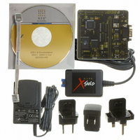
DEV KIT FOR Z16F ZNEO
Manufacturer
Zilog
Series
ZNEO™r
Type
MCUr
Datasheets
1.Z16F2800100ZCOG.pdf
(2 pages)
2.Z16F2800100ZCOG.pdf
(30 pages)
3.Z16F2800100ZCOG.pdf
(388 pages)
Specifications of Z16F2800100ZCOG
Contents
Evaluation Board, Software and Documentation
For Use With/related Products
Z16F Series
For Use With
269-4661 - KIT ACC ETHERNET SMART CABLE
Lead Free Status / RoHS Status
Lead free / RoHS Compliant
Other names
269-4537


®
ZNEO
Z16F Series
Product Specification
187
Multi-Master SPI Operation
In a multi-master SPI system, all SCK pins are tied together, all MOSI pins are tied
together and all MISO pins are tied together. All SPI pins must be configured in open-
drain mode to prevent bus contention. At any time, only one SPI device is configured as
the master and all other devices on the bus are configured as slaves. The master asserts the
SS pin on the selected slave. Then, the active master drives the clock and transmit data on
the SCK and MOSI pins to the SCK and MOSI pins on the slave (including those slaves
which are not enabled). The enabled slave drives data out its MISO pin to the MISO
master pin.
When the ESPI is configured as a master in a multi-master SPI system, the SS pin must be
configured as an input. The SS input signal on a device configured as a master must
remain High. If the SS signal on the active master goes Low (indicating another master is
accessing this device as a slave), a collision error flag is set in the ESPI status register. The
slave select outputs on a master in a multi-master system must come from GPIO pins.
SPI Slave Operation
The ESPI block is configured for SLAVE mode operation by setting the MMEN bit = 0 in
the ESPICTL register and setting the
bit
in the ESPIMODE register. The SSMD
SSIO
= 0
field of the ESPI mode register is set to 00 for SPI protocol mode. The
,
and
Phase
Clkpol
bits in the ESPICTL register and the NUMBITS field in the ESPIMODE register must
WOR
be set to be consistent with the other SPI devices. Typically for an SPI slave SSPO = 0.
If the slave has data to send to the master, the data must be written to the data register
before the transaction starts (first edge of SCK when SS is asserted). If the data register is
not written prior to the slave transaction, the MISO pin outputs all 1s.
Due to the delay resulting from synchronization of the SS and SCK input signals to the
internal system clock, the maximum SCK baud rate which is supported in SLAVE mode is
the system clock frequency divided by 8. This rate is controlled by the SPI master.
Figure 41
on page 188 displays the ESPI configuration in SPI SLAVE mode.
PS022008-0810
P R E L I M I N A R Y
Enhanced Serial Peripheral Interface
Related parts for Z16F2800100ZCOG
Image
Part Number
Description
Manufacturer
Datasheet
Request
R

Part Number:
Description:
Communication Controllers, ZILOG INTELLIGENT PERIPHERAL CONTROLLER (ZIP)
Manufacturer:
Zilog, Inc.
Datasheet:

Part Number:
Description:
KIT DEV FOR Z8 ENCORE 16K TO 64K
Manufacturer:
Zilog
Datasheet:

Part Number:
Description:
KIT DEV Z8 ENCORE XP 28-PIN
Manufacturer:
Zilog
Datasheet:

Part Number:
Description:
DEV KIT FOR Z8 ENCORE 8K/4K
Manufacturer:
Zilog
Datasheet:

Part Number:
Description:
KIT DEV Z8 ENCORE XP 28-PIN
Manufacturer:
Zilog
Datasheet:

Part Number:
Description:
DEV KIT FOR Z8 ENCORE 4K TO 8K
Manufacturer:
Zilog
Datasheet:
Part Number:
Description:
CMOS Z8 microcontroller. ROM 16 Kbytes, RAM 256 bytes, speed 16 MHz, 32 lines I/O, 3.0V to 5.5V
Manufacturer:
Zilog, Inc.
Datasheet:
Part Number:
Description:
Low-cost microcontroller. 512 bytes ROM, 61 bytes RAM, 8 MHz
Manufacturer:
Zilog, Inc.
Datasheet:
Part Number:
Description:
Z8 4K OTP Microcontroller
Manufacturer:
Zilog, Inc.
Datasheet:
Part Number:
Description:
CMOS SUPER8 ROMLESS MCU
Manufacturer:
Zilog, Inc.
Datasheet:
Part Number:
Description:
SL1866 CMOSZ8 OTP Microcontroller
Manufacturer:
Zilog, Inc.
Datasheet:
Part Number:
Description:
SL1866 CMOSZ8 OTP Microcontroller
Manufacturer:
Zilog, Inc.
Datasheet:
Part Number:
Description:
OTP (KB) = 1, RAM = 125, Speed = 12, I/O = 14, 8-bit Timers = 2, Comm Interfaces Other Features = Por, LV Protect, Voltage = 4.5-5.5V
Manufacturer:
Zilog, Inc.
Datasheet:
Part Number:
Description:
Manufacturer:
Zilog, Inc.
Datasheet: