Z16F2800100ZCOG Zilog, Z16F2800100ZCOG Datasheet - Page 311
Z16F2800100ZCOG
Manufacturer Part Number
Z16F2800100ZCOG
Description
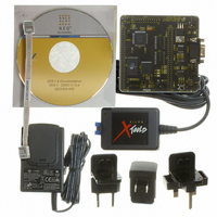
DEV KIT FOR Z16F ZNEO
Manufacturer
Zilog
Series
ZNEO™r
Type
MCUr
Datasheets
1.Z16F2800100ZCOG.pdf
(2 pages)
2.Z16F2800100ZCOG.pdf
(30 pages)
3.Z16F2800100ZCOG.pdf
(388 pages)
Specifications of Z16F2800100ZCOG
Contents
Evaluation Board, Software and Documentation
For Use With/related Products
Z16F Series
For Use With
269-4661 - KIT ACC ETHERNET SMART CABLE
Lead Free Status / RoHS Status
Lead free / RoHS Compliant
Other names
269-4537


Table 159. Options Bits at Program Memory Address 0001H
PS022008-0810
BITS
FIELD
RESET
R/W
ADDR
Note: U = Unchanged by Reset. R/W = Read/Write.
Program Memory Address 0001H
R/W
U
7
FWP—Flash Write Protect
RP—Read Protect
0 = User program code is inaccessible. Limited control features are available through the
OCD.
1 = User program code is accessible. All OCD commands are enabled. This setting is the
default for unprogrammed (erased) Flash.
Option bits in this space are altered to change the chip configuration at reset.
Reserved
These Option Bits are reserved for future use and must always be 1. This setting is the
default for unprogrammed (erased) Flash.
MCEN—Motor control enable
0 = Motor control pins are enabled on reset
1 = Normal Pin operation
PWMHI—
0 = The high side off value is equal to zero.
1 = The high side off value is equal to one.
PWMLO
0 = The low side off value is equal to zero.
1 = The low side off value is equal to one.
FWP
0
1
—Low side off initial value
R/W
High side off initial value
Description
Programming, Page Erase, and Mass Erase through user code is disabled. Flash
operations are allowed through the On-Chip Debugger
Programming, Page Erase, and Mass Erase are enabled for all of Flash Program
Memory.
U
6
Reserved
R/W
U
5
P R E L I M I N A R Y
Program Memory 0001H
R/W
U
4
R/W
U
3
MCEN
R/W
U
2
Product Specification
ZNEO
PWMHI
R/W
U
1
Z16F Series
Option Bits
PWMLO
R/W
U
0
295
Related parts for Z16F2800100ZCOG
Image
Part Number
Description
Manufacturer
Datasheet
Request
R

Part Number:
Description:
Communication Controllers, ZILOG INTELLIGENT PERIPHERAL CONTROLLER (ZIP)
Manufacturer:
Zilog, Inc.
Datasheet:

Part Number:
Description:
KIT DEV FOR Z8 ENCORE 16K TO 64K
Manufacturer:
Zilog
Datasheet:

Part Number:
Description:
KIT DEV Z8 ENCORE XP 28-PIN
Manufacturer:
Zilog
Datasheet:

Part Number:
Description:
DEV KIT FOR Z8 ENCORE 8K/4K
Manufacturer:
Zilog
Datasheet:

Part Number:
Description:
KIT DEV Z8 ENCORE XP 28-PIN
Manufacturer:
Zilog
Datasheet:

Part Number:
Description:
DEV KIT FOR Z8 ENCORE 4K TO 8K
Manufacturer:
Zilog
Datasheet:
Part Number:
Description:
CMOS Z8 microcontroller. ROM 16 Kbytes, RAM 256 bytes, speed 16 MHz, 32 lines I/O, 3.0V to 5.5V
Manufacturer:
Zilog, Inc.
Datasheet:
Part Number:
Description:
Low-cost microcontroller. 512 bytes ROM, 61 bytes RAM, 8 MHz
Manufacturer:
Zilog, Inc.
Datasheet:
Part Number:
Description:
Z8 4K OTP Microcontroller
Manufacturer:
Zilog, Inc.
Datasheet:
Part Number:
Description:
CMOS SUPER8 ROMLESS MCU
Manufacturer:
Zilog, Inc.
Datasheet:
Part Number:
Description:
SL1866 CMOSZ8 OTP Microcontroller
Manufacturer:
Zilog, Inc.
Datasheet:
Part Number:
Description:
SL1866 CMOSZ8 OTP Microcontroller
Manufacturer:
Zilog, Inc.
Datasheet:
Part Number:
Description:
OTP (KB) = 1, RAM = 125, Speed = 12, I/O = 14, 8-bit Timers = 2, Comm Interfaces Other Features = Por, LV Protect, Voltage = 4.5-5.5V
Manufacturer:
Zilog, Inc.
Datasheet:
Part Number:
Description:
Manufacturer:
Zilog, Inc.
Datasheet: