Z16F2800100ZCOG Zilog, Z16F2800100ZCOG Datasheet - Page 30
Z16F2800100ZCOG
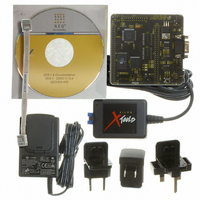
Manufacturer Part Number
Z16F2800100ZCOG
Description
DEV KIT FOR Z16F ZNEO
Manufacturer
Zilog
Series
ZNEO™r
Type
MCUr
Datasheets
1.Z16F2800100ZCOG.pdf
(2 pages)
2.Z16F2800100ZCOG.pdf
(30 pages)
3.Z16F2800100ZCOG.pdf
(388 pages)
Specifications of Z16F2800100ZCOG
Contents
Evaluation Board, Software and Documentation
For Use With/related Products
Z16F Series
For Use With
269-4661 - KIT ACC ETHERNET SMART CABLE
Lead Free Status / RoHS Status
Lead free / RoHS Compliant
Other names
269-4537


Table 2. Signal Descriptions (Continued)
PS022008-0810
Signal Mnemonic
CINP
CINN
COMPOUT
OPINP
OPINN
OPOUT
Oscillators
XIN
XOUT
On-Chip Debugger
DBG
Reset
RESET
Power Supply
VDD
AVDD
VSS
AVSS
Caution:
I/O
I/O
I/O
O
O
O
I
I
I
I
I
I
I
I
I
Description
Comparator positive input
Comparator negative input
Comparator output
Operational amplifier positive input
Operational amplifier negative input
Operational amplifier output
External crystal input: This is the input pin to the crystal
oscillator.
A crystal is connected between it and the
oscillator. In addition, this pin is used with external RC networks or
external clock drivers to provide the system clock to the system.
External crystal output: This pin is the output of crystal oscillator.
A crystal is con nected between it an d the
oscillator. This pin must be left unconnected when not us ing a
crystal.
Debug: This pin is the control and data input and output to an d
from the OCD.
For operation of the OCD, all power pins (VDD and AVDD) must
be supplied with power and all ground pins (VSS and AVSS) must
be grounded. This pin is open-drain and must have an external
pull-up resistor to ensure proper operation.
RESET: Bidirectional RESET signals generates a Reset whe n
asserted (driven Low) and drives a Low output when the ZNEO is
in Reset.
Power supply
Analog power supply
Ground
Analog ground
P R E L I M I N A R Y
Signal and Pin Descriptions
Product Specification
XOUT
ZNEO
XIN
pin to form the
pin to form the
Z16F Series
15
Related parts for Z16F2800100ZCOG
Image
Part Number
Description
Manufacturer
Datasheet
Request
R

Part Number:
Description:
Communication Controllers, ZILOG INTELLIGENT PERIPHERAL CONTROLLER (ZIP)
Manufacturer:
Zilog, Inc.
Datasheet:

Part Number:
Description:
KIT DEV FOR Z8 ENCORE 16K TO 64K
Manufacturer:
Zilog
Datasheet:

Part Number:
Description:
KIT DEV Z8 ENCORE XP 28-PIN
Manufacturer:
Zilog
Datasheet:

Part Number:
Description:
DEV KIT FOR Z8 ENCORE 8K/4K
Manufacturer:
Zilog
Datasheet:

Part Number:
Description:
KIT DEV Z8 ENCORE XP 28-PIN
Manufacturer:
Zilog
Datasheet:

Part Number:
Description:
DEV KIT FOR Z8 ENCORE 4K TO 8K
Manufacturer:
Zilog
Datasheet:
Part Number:
Description:
CMOS Z8 microcontroller. ROM 16 Kbytes, RAM 256 bytes, speed 16 MHz, 32 lines I/O, 3.0V to 5.5V
Manufacturer:
Zilog, Inc.
Datasheet:
Part Number:
Description:
Low-cost microcontroller. 512 bytes ROM, 61 bytes RAM, 8 MHz
Manufacturer:
Zilog, Inc.
Datasheet:
Part Number:
Description:
Z8 4K OTP Microcontroller
Manufacturer:
Zilog, Inc.
Datasheet:
Part Number:
Description:
CMOS SUPER8 ROMLESS MCU
Manufacturer:
Zilog, Inc.
Datasheet:
Part Number:
Description:
SL1866 CMOSZ8 OTP Microcontroller
Manufacturer:
Zilog, Inc.
Datasheet:
Part Number:
Description:
SL1866 CMOSZ8 OTP Microcontroller
Manufacturer:
Zilog, Inc.
Datasheet:
Part Number:
Description:
OTP (KB) = 1, RAM = 125, Speed = 12, I/O = 14, 8-bit Timers = 2, Comm Interfaces Other Features = Por, LV Protect, Voltage = 4.5-5.5V
Manufacturer:
Zilog, Inc.
Datasheet:
Part Number:
Description:
Manufacturer:
Zilog, Inc.
Datasheet: