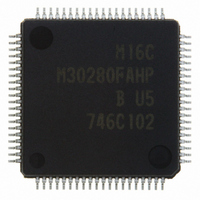
M30280FAHP#U5B Renesas Electronics America, M30280FAHP#U5B Datasheet - Page 199

M30280FAHP#U5B
Manufacturer Part Number
M30280FAHP#U5B
Description
IC M16C/28 MCU FLASH 96K 80LQFP
Manufacturer
Renesas Electronics America
Series
M16C™ M16C/Tiny/28r
Specifications of M30280FAHP#U5B
Core Size
16-Bit
Program Memory Size
96KB (96K x 8)
Core Processor
M16C/60
Speed
20MHz
Connectivity
I²C, IEBus, SIO, UART/USART
Peripherals
DMA, POR, PWM, Voltage Detect, WDT
Number Of I /o
71
Program Memory Type
FLASH
Ram Size
8K x 8
Voltage - Supply (vcc/vdd)
2.7 V ~ 5.5 V
Data Converters
A/D 24x10b
Oscillator Type
Internal
Operating Temperature
-20°C ~ 85°C
Package / Case
80-LQFP
Controller Family/series
M16C
No. Of I/o's
71
Ram Memory Size
8KB
Cpu Speed
20MHz
No. Of Timers
10
Digital Ic Case Style
LQFP
Embedded Interface Type
I2C, UART
Rohs Compliant
Yes
Lead Free Status / RoHS Status
Lead free / RoHS Compliant
For Use With
R0K330290S000BE - KIT EVAL STARTER FOR M16C/29M30290T2-CPE - EMULATOR COMPACT M16C/26A/28/29M30290T2-CPE-HP - EMULATOR COMPACT FOR M16C/TINY
Eeprom Size
-
Lead Free Status / RoHS Status
Lead free / RoHS Compliant, Lead free / RoHS Compliant
Available stocks
Company
Part Number
Manufacturer
Quantity
Price
- Current page: 199 of 425
- Download datasheet (4Mb)
M
R
R
1
e
E
Table 14.3 Pin Functions (When Not Select Multiple Transfer Clock Output Pin Function)
Table 14.4 P6
NOTES:
NOTES:
. v
6
J
TxDi (i = 0 to 2)
(P6
RxDi
(P6
CLKi
(P6
CTSi/RTSi
(P6
0
C
2
1: When the U1MAP bit in PACR register is “1” (P7
9
Pin name
Table 14.3 lists pin functions for the case where the multiple transfer clock output pin select function is
deselected. Table 14.4 lists the P6
Note that for a period from when the UARTi operation mode is selected to when transfer starts, the TxDi
pin outputs an “H”. (If the N-channel open-drain output is selected, this pin is in a high-impedance state.)
P6
2 /
Pin function
CTS
RTS
CTS
CLKS
0 .
B
3
2
1
0
, P6
, P6
, P6
, P6
8
0
0
4
0
1. When the U1MAP bit in PACR register is “1” (P7
2. In addition to this, set the CRD bit in the U0C0 register to “0” (CT0
3. When the CLKMD1 bit is set to "1" and the CLKMD0 bit is set to "0", the following logiclevels
G
4
J
0 (2)
7
1
1
6
5
4
• High if the CLKPOL bit in the U1C0 register is set to "0"
• Low if the CLKPOL bit in the U1C0 register is set to "1"
7
a
o r
, P7
, P7
, P7
, P7
CRS bit in the U0C0 register to “1” (RTS
1
0 -
. n
are output:
u
2
p
0
3
3
1
2
0
)
)
)
)
, 1
0
(
Serial data output
Serial data input
CTS input
M
Transfer clock output
Transfer clock input
RTS output
I/O port
4
2
1
0
Pin Functions
0
6
7
C
CRD
U1C0 register
2 /
Function
1
0
0
0
, 8
page 177
M
1
6
CRS
C
0
1
0
2 /
f o
(1)
8
3
) B
8
5
(Outputs dummy data when performing reception only)
Set the CKDIR bit in the UiMR register to "0"
Set the PD6_2 bit and PD6_6 bit in the PD6 register, and PD7_1 bit in the PD7
register to "0"(Can be used as an input port when performing transmission only)
Set the CRD bit in the UiC0 register to "0"
Set the CRS bit in the UiC0 register to "0"
Set the PD6_0 bit and PD6_4 bit in the PD6 register is set to "0", the PD7_3 bit
in the PD7 register to "0"
Set the CKDIR bit in the UiMR register to "1"
Set the PD6_1 bit and PD6_5 bit in the PD6 register, and the PD7_2 bit in the
PD7 register to "0"
Set the CRD bit in the UiC0 register to "0"
Set the CRS bit in the UiC0 register to "1"
Set the CRD bit in the UiC0 register to "1"
4
RCSP
pin functions during clock synchronous serial I/O mode.
1
0
0
0
Bit set value
3
to P7
UCON register
0
1
CLKMD1
0
), UART1 pin is assgined to P7
(3)
selected).
0
0
0
0
3
to P7
Method of selection
CLKMD0
0
1
), this table lists the P7
Input: 0, Output: 1
0
0
3
0
to P7
/RT0
PD6 register
0
PD6_4
.
0
enabled) and the
0
functions.
(1)
14. Serial I/O
Related parts for M30280FAHP#U5B
Image
Part Number
Description
Manufacturer
Datasheet
Request
R

Part Number:
Description:
KIT STARTER FOR M16C/29
Manufacturer:
Renesas Electronics America
Datasheet:

Part Number:
Description:
KIT STARTER FOR R8C/2D
Manufacturer:
Renesas Electronics America
Datasheet:

Part Number:
Description:
R0K33062P STARTER KIT
Manufacturer:
Renesas Electronics America
Datasheet:

Part Number:
Description:
KIT STARTER FOR R8C/23 E8A
Manufacturer:
Renesas Electronics America
Datasheet:

Part Number:
Description:
KIT STARTER FOR R8C/25
Manufacturer:
Renesas Electronics America
Datasheet:

Part Number:
Description:
KIT STARTER H8S2456 SHARPE DSPLY
Manufacturer:
Renesas Electronics America
Datasheet:

Part Number:
Description:
KIT STARTER FOR R8C38C
Manufacturer:
Renesas Electronics America
Datasheet:

Part Number:
Description:
KIT STARTER FOR R8C35C
Manufacturer:
Renesas Electronics America
Datasheet:

Part Number:
Description:
KIT STARTER FOR R8CL3AC+LCD APPS
Manufacturer:
Renesas Electronics America
Datasheet:

Part Number:
Description:
KIT STARTER FOR RX610
Manufacturer:
Renesas Electronics America
Datasheet:

Part Number:
Description:
KIT STARTER FOR R32C/118
Manufacturer:
Renesas Electronics America
Datasheet:

Part Number:
Description:
KIT DEV RSK-R8C/26-29
Manufacturer:
Renesas Electronics America
Datasheet:

Part Number:
Description:
KIT STARTER FOR SH7124
Manufacturer:
Renesas Electronics America
Datasheet:

Part Number:
Description:
KIT STARTER FOR H8SX/1622
Manufacturer:
Renesas Electronics America
Datasheet:

Part Number:
Description:
KIT DEV FOR SH7203
Manufacturer:
Renesas Electronics America
Datasheet:


