M30280FAHP#U5B Renesas Electronics America, M30280FAHP#U5B Datasheet - Page 237
M30280FAHP#U5B
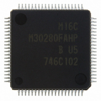
Manufacturer Part Number
M30280FAHP#U5B
Description
IC M16C/28 MCU FLASH 96K 80LQFP
Manufacturer
Renesas Electronics America
Series
M16C™ M16C/Tiny/28r
Specifications of M30280FAHP#U5B
Core Size
16-Bit
Program Memory Size
96KB (96K x 8)
Core Processor
M16C/60
Speed
20MHz
Connectivity
I²C, IEBus, SIO, UART/USART
Peripherals
DMA, POR, PWM, Voltage Detect, WDT
Number Of I /o
71
Program Memory Type
FLASH
Ram Size
8K x 8
Voltage - Supply (vcc/vdd)
2.7 V ~ 5.5 V
Data Converters
A/D 24x10b
Oscillator Type
Internal
Operating Temperature
-20°C ~ 85°C
Package / Case
80-LQFP
Controller Family/series
M16C
No. Of I/o's
71
Ram Memory Size
8KB
Cpu Speed
20MHz
No. Of Timers
10
Digital Ic Case Style
LQFP
Embedded Interface Type
I2C, UART
Rohs Compliant
Yes
Lead Free Status / RoHS Status
Lead free / RoHS Compliant
For Use With
R0K330290S000BE - KIT EVAL STARTER FOR M16C/29M30290T2-CPE - EMULATOR COMPACT M16C/26A/28/29M30290T2-CPE-HP - EMULATOR COMPACT FOR M16C/TINY
Eeprom Size
-
Lead Free Status / RoHS Status
Lead free / RoHS Compliant, Lead free / RoHS Compliant
Available stocks
Company
Part Number
Manufacturer
Quantity
Price


M
R
R
1
e
E
. v
6
Figure 14.38 Polarity of Transfer Clock
Figure 14.37 SI/Oi Operation Timing
J
0
C
14.2.1 SI/Oi Operation Timing
14.2.2 CLK Polarity Selection
2
9
2 /
Figure 14.37 shows the SI/Oi operation timing
The the SMi4 bit in the SiC register allows selection of the polarity of the transfer clock. Figure 14.38
shows the polarity of the transfer clock.
0 .
B
8
0
0
NOTES:
Signal written to the
SI/Oi internal clock
0
G
4
J
1. This diagram applies to the case where the SiC register bits are set as follows:
2. When the SMi6 bit is set to "1" (internal clock), the S
3. If the SMi6 bit is set to "0" (internal clock), the serial I/O starts sending or receiving data a maximum of 1.5 transfer clock cycles after writing to
7
a
o r
SMi2=0 (S
rising edge of the transfer clock), SMi5=0 (LSB first) and SMi6=1 (internal clock)
the SiTRR register.
SiTRR register
0 -
S
. n
SiIC register
i= 3, 4
OUT
u
CLKi output
2
p
S
3
0
IN
, 1
i output
0
(
i input
M
IR bit
(2) When the SMi4 bit in the SiC register is set to “1”
(1) When the SMi4 bit in the SiC register is set to “0”
CLK
S
S
CLK
S
S
NOTES:
2
OUT
i=3 and 4
INi
OUTi
INi
OUTi
1
0
6
0
1. This diagram applies to the case where the SiC register bits are set as follows:
2. When the SMi6 bit is set to "1" (internal clock), a high level is output from the CLKi
3 When the SMi6 bit is set to "1" (internal clock), a low level is output from the CLKi
i output), SMi3=1 (S
i
i
7
C
pin if not transferring data.
pin if not transferring data.
SMi5=0 (LSB first) and SMi6=1 (internal clock)
2 /
"H"
"H"
"L"
"L"
"H"
"H"
"H"
"L"
"L"
"L"
"1"
"0"
, 8
page 215
M
1
6
1.5 cycle (max)
D0
D
D
D
C
0
0
0
OUT
2 /
f o
8
i output, CLKi function), SMi4=0 (transmit data output at the falling edge and receive data input at the
3
) B
D
D
D
D
8
1
1
1
1
5
(3)
D
D
D
D
2
2
2
2
D
0
OUT
D
D
D
D
i pin is placed in the high-impedance state after the transfer is completed.
3
3
3
3
D
1
D
D
D
D
4
4
4
4
D
D
D
D
D
2
5
5
5
5
D
D
D
D
6
6
6
6
D
3
D
D
D
D
7
7
7
7
D
4
(3)
(2)
D
5
D
6
D
7
(2)
14. Serial I/O
Related parts for M30280FAHP#U5B
Image
Part Number
Description
Manufacturer
Datasheet
Request
R

Part Number:
Description:
KIT STARTER FOR M16C/29
Manufacturer:
Renesas Electronics America
Datasheet:

Part Number:
Description:
KIT STARTER FOR R8C/2D
Manufacturer:
Renesas Electronics America
Datasheet:

Part Number:
Description:
R0K33062P STARTER KIT
Manufacturer:
Renesas Electronics America
Datasheet:

Part Number:
Description:
KIT STARTER FOR R8C/23 E8A
Manufacturer:
Renesas Electronics America
Datasheet:

Part Number:
Description:
KIT STARTER FOR R8C/25
Manufacturer:
Renesas Electronics America
Datasheet:

Part Number:
Description:
KIT STARTER H8S2456 SHARPE DSPLY
Manufacturer:
Renesas Electronics America
Datasheet:

Part Number:
Description:
KIT STARTER FOR R8C38C
Manufacturer:
Renesas Electronics America
Datasheet:

Part Number:
Description:
KIT STARTER FOR R8C35C
Manufacturer:
Renesas Electronics America
Datasheet:

Part Number:
Description:
KIT STARTER FOR R8CL3AC+LCD APPS
Manufacturer:
Renesas Electronics America
Datasheet:
Part Number:
Description:
KIT STARTER FOR RX610
Manufacturer:
Renesas Electronics America
Datasheet:

Part Number:
Description:
KIT STARTER FOR R32C/118
Manufacturer:
Renesas Electronics America
Datasheet:

Part Number:
Description:
KIT DEV RSK-R8C/26-29
Manufacturer:
Renesas Electronics America
Datasheet:

Part Number:
Description:
KIT STARTER FOR SH7124
Manufacturer:
Renesas Electronics America
Datasheet:

Part Number:
Description:
KIT STARTER FOR H8SX/1622
Manufacturer:
Renesas Electronics America
Datasheet:

Part Number:
Description:
KIT DEV FOR SH7203
Manufacturer:
Renesas Electronics America
Datasheet: