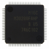
M30280FAHP#U5B Renesas Electronics America, M30280FAHP#U5B Datasheet - Page 304
M30280FAHP#U5B
Manufacturer Part Number
M30280FAHP#U5B
Description
IC M16C/28 MCU FLASH 96K 80LQFP
Manufacturer
Renesas Electronics America
Series
M16C™ M16C/Tiny/28r
Specifications of M30280FAHP#U5B
Core Size
16-Bit
Program Memory Size
96KB (96K x 8)
Core Processor
M16C/60
Speed
20MHz
Connectivity
I²C, IEBus, SIO, UART/USART
Peripherals
DMA, POR, PWM, Voltage Detect, WDT
Number Of I /o
71
Program Memory Type
FLASH
Ram Size
8K x 8
Voltage - Supply (vcc/vdd)
2.7 V ~ 5.5 V
Data Converters
A/D 24x10b
Oscillator Type
Internal
Operating Temperature
-20°C ~ 85°C
Package / Case
80-LQFP
Controller Family/series
M16C
No. Of I/o's
71
Ram Memory Size
8KB
Cpu Speed
20MHz
No. Of Timers
10
Digital Ic Case Style
LQFP
Embedded Interface Type
I2C, UART
Rohs Compliant
Yes
Lead Free Status / RoHS Status
Lead free / RoHS Compliant
For Use With
R0K330290S000BE - KIT EVAL STARTER FOR M16C/29M30290T2-CPE - EMULATOR COMPACT M16C/26A/28/29M30290T2-CPE-HP - EMULATOR COMPACT FOR M16C/TINY
Eeprom Size
-
Lead Free Status / RoHS Status
Lead free / RoHS Compliant, Lead free / RoHS Compliant
Available stocks
Company
Part Number
Manufacturer
Quantity
Price


M
R
R
17. Programmable I/O Ports
17.1 Port Pi Direction Register (PDi Register, i = 0 to 3, 6 to 10)
17.2 Port Pi Register (Pi Register, i = 0 to 3, 6 to 10)
17.3 Pull-up Control Register 0 to 2 (PUR0 to PUR2 Registers)
17.4 Port Control Register (PCR Register)
e
E
1
. v
J
6
The programmable input/output ports (hereafter referred to simply as “I/O ports”) consist of 71 lines P0,
P1,P2, P3, P6, P7, P8, P9, P10 (except P9
P3
every line by using a direction register, and can also be chosen to be or not be pulled high in sets of 4 lines.
Figures 17.1 to 17.4 show the I/O ports. Figure 17.5 shows the I/O pins.
Each pin functions as an I/O port, a peripheral function input/output.
For details on how to set peripheral functions, refer to each functional description in this manual. If any pin
is used as a peripheral function input, set the direction bit for that pin to “0” (input mode). Any pin used as an
output pin for peripheral functions is directed for output no matter how the corresponding direction bit is set.
Figure 17.6 shows the direction registers.
This register selects whether the I/O port is to be used for input or output. The bits in this register corre-
spond one for one to each port.
Figure 17.7 shows the Pi registers.
Data input/output to and from external devices are accomplished by reading and writing to the Pi register.
The Pi register consists of a port latch to hold the output data and a circuit to read the pin status. For ports
set for input mode, the input level of the pin can be read by reading the corresponding Pi register, and data
can be written to the port latch by writing to the Pi register.
For ports set for output mode, the port latch can be read by reading the corresponding Pi register, and data
can be written to the port latch by writing to the Pi register. The data written to the port latch is output from
the pin. The bits in the Pi register correspond one for one to each port.
Figure 17.8 shows the PUR0 to PUR2 registers.
Registers PUR0 to PUR2 select whether the ports, divided into groups of four ports, are pulled up or not.
The ports, selected by setting the bits in registers PUR2 to PUR0 to “1” (pull-up), are pulled up when the
direction registers are set to “0” (input mode). The ports are pulled up regardless of their function.
Figure 17.9 shows the port control register.
When the P1 register is read after setting the PCR0 bit in the PCR register to “1”, the corresponding port
latch can be read no matter how the PD1 register is set.
0
C
2
9
2 /
0 .
B
0
Note
Ports P0
package).
0
0
8
to P3
0
G
4
J
7
a
o r
0 -
. n
u
3
2
3
p
, P6, P7, P8, P9
0
, 1
4
0
(
M
to P0
2
0
1
0
6
7
C
2 /
7
, P1
page 282
, 8
M
0
1
to P1
6
0
C
to P9
2 /
f o
8
4
3
) B
8
, P3
3
5
, P10 for the 64-pin package. Each port can be set for input or output
4
to P3
4
) for the 80-pin package, or 55 lines P0
7
and P9
5
to P9
7
are not available in M16C/28 (64-pin
17. Programmable I/O Ports
0
to P0
3
, P1
5
to P1
7
, P2,
Related parts for M30280FAHP#U5B
Image
Part Number
Description
Manufacturer
Datasheet
Request
R

Part Number:
Description:
KIT STARTER FOR M16C/29
Manufacturer:
Renesas Electronics America
Datasheet:

Part Number:
Description:
KIT STARTER FOR R8C/2D
Manufacturer:
Renesas Electronics America
Datasheet:

Part Number:
Description:
R0K33062P STARTER KIT
Manufacturer:
Renesas Electronics America
Datasheet:

Part Number:
Description:
KIT STARTER FOR R8C/23 E8A
Manufacturer:
Renesas Electronics America
Datasheet:

Part Number:
Description:
KIT STARTER FOR R8C/25
Manufacturer:
Renesas Electronics America
Datasheet:

Part Number:
Description:
KIT STARTER H8S2456 SHARPE DSPLY
Manufacturer:
Renesas Electronics America
Datasheet:

Part Number:
Description:
KIT STARTER FOR R8C38C
Manufacturer:
Renesas Electronics America
Datasheet:

Part Number:
Description:
KIT STARTER FOR R8C35C
Manufacturer:
Renesas Electronics America
Datasheet:

Part Number:
Description:
KIT STARTER FOR R8CL3AC+LCD APPS
Manufacturer:
Renesas Electronics America
Datasheet:
Part Number:
Description:
KIT STARTER FOR RX610
Manufacturer:
Renesas Electronics America
Datasheet:

Part Number:
Description:
KIT STARTER FOR R32C/118
Manufacturer:
Renesas Electronics America
Datasheet:

Part Number:
Description:
KIT DEV RSK-R8C/26-29
Manufacturer:
Renesas Electronics America
Datasheet:

Part Number:
Description:
KIT STARTER FOR SH7124
Manufacturer:
Renesas Electronics America
Datasheet:

Part Number:
Description:
KIT STARTER FOR H8SX/1622
Manufacturer:
Renesas Electronics America
Datasheet:

Part Number:
Description:
KIT DEV FOR SH7203
Manufacturer:
Renesas Electronics America
Datasheet: