M30280FAHP#U5B Renesas Electronics America, M30280FAHP#U5B Datasheet - Page 388
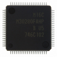
M30280FAHP#U5B
Manufacturer Part Number
M30280FAHP#U5B
Description
IC M16C/28 MCU FLASH 96K 80LQFP
Manufacturer
Renesas Electronics America
Series
M16C™ M16C/Tiny/28r
Specifications of M30280FAHP#U5B
Core Size
16-Bit
Program Memory Size
96KB (96K x 8)
Core Processor
M16C/60
Speed
20MHz
Connectivity
I²C, IEBus, SIO, UART/USART
Peripherals
DMA, POR, PWM, Voltage Detect, WDT
Number Of I /o
71
Program Memory Type
FLASH
Ram Size
8K x 8
Voltage - Supply (vcc/vdd)
2.7 V ~ 5.5 V
Data Converters
A/D 24x10b
Oscillator Type
Internal
Operating Temperature
-20°C ~ 85°C
Package / Case
80-LQFP
Controller Family/series
M16C
No. Of I/o's
71
Ram Memory Size
8KB
Cpu Speed
20MHz
No. Of Timers
10
Digital Ic Case Style
LQFP
Embedded Interface Type
I2C, UART
Rohs Compliant
Yes
Lead Free Status / RoHS Status
Lead free / RoHS Compliant
For Use With
R0K330290S000BE - KIT EVAL STARTER FOR M16C/29M30290T2-CPE - EMULATOR COMPACT M16C/26A/28/29M30290T2-CPE-HP - EMULATOR COMPACT FOR M16C/TINY
Eeprom Size
-
Lead Free Status / RoHS Status
Lead free / RoHS Compliant, Lead free / RoHS Compliant
Available stocks
Company
Part Number
Manufacturer
Quantity
Price


M
R
R
e
E
1
. v
Table 20.1 Uses of IT Bit in the G1BCR0 Register and G1BTRR Register
J
6
1
0
0
20.7.2 Rewrite the ICOCiIC Register
20.7.3 Waveform Generating Function
20.7.4 IC/OC Base Timer Interrupt
C
2
b (
9
b (
2 /
When the interrupt request to the ICOCiIC register is generated during the instruction process, the IR bit
may not be set to "1" (interrupt requested) and the interrupt request may not be acknowledged. At that
time, when the bit in the G1IR register is held to "1" (interrupt requested), the following IC/OC interrupt
request will not be generated. When changing the ICOCiIC register settiing, use the following instruction.
When initializing Timer S, change the ICOCiIC register setting with the request again after setting the
IOCiIC and G1IR registers to "00
1. If the BTS bit in the G1BCR1 register is set to "0" (base timer is reset) when the waveform is generating
and the base timer is stopped counting, the waveform output pin keeps the same output level. The output
level will be changed when the base timer and the G1POj register match the setting value next time after
the base timer starts counting again.
2. If the G1POCRj register is set when the waveform is generated, the same setting value of the IVL bit is
applied to the waveform generating pin. Do not set the G1POCRj register when the waveform is generat-
ing.
3. When the RST1 bit in the G1BCR1 register is set to "1" (the base timer is reset by matching the G1PO0
If the MCU is operated in the combination selected from Tabl e 1 for use when the RST4 bit in the
G1BCR0 register is set to 1 (reset the base timer that matches the G1BTRR register) to reset the base
timer, an IC/OC base timer interrupt request is generated twice.
The second IC/OC base timer interrupt request is generated because the base timer overflow request is
generated after one fBT1 clock cycle as soon as the base timer is reset.
One of the following conditions must be met in order not to generate the IC/OC base timer interrupt
request twice:
1) When the RST4 bit is set to 1, set the G1BTRR register with a combination other than what is listed in
2) Do not reset the base timer by matching the G1BTRR register. Reset the base timer by matching the
0 .
B
t i
t i
0
0
register), the base timer is reset after two clock cycles of f
G1PO0 register value. A high-level ("H") signal is applied to the OUTC10 pin between the base timer
value match to the base timer reset.
8
1
1
Table 20.1.
G1P00 register. In other words, do not set the RST4 bit to 1 to reset the base timer. Set the RST1 bit in
the G1BCR1 register to 1 (reset the base timer that matches the G1P00 register).
0
Subject instructions: AND, OR, BCLR, BSET
5
4
G
4
J
n i
n i
7
a
o r
0 -
. n
h t
h t
T I
u
2
e
e
3
p
0
B
b
b
, 1
0
t i
a
a
(
M
s
s
n i
2
e
e
0
1
h t
i t
i t
0
6
m
m
e
7
C
r e
r e
G
2 /
1
o
o
page 366
B
, 8
v
v
C
e
e
f r
f r
R
M
o l
o l
0
1
w
w
R
6
) s
) s
e
C
g
t s i
2 /
f o
r e
8
3
) B
8
5
16
".
0
3
0
0
G
F
B
7
F
F
F
1
F
F
F
B
F
1
F
T
6
1
1
R
6
6
o t
R
o t
o t
0
R
F
0
0
e
F
F
F
g
F
F
F
BT1
t s i
E
F
F
E
r e
1
E
6
1
1
6
6
r o
when the base timer value matches the
20. Precautions
Related parts for M30280FAHP#U5B
Image
Part Number
Description
Manufacturer
Datasheet
Request
R

Part Number:
Description:
KIT STARTER FOR M16C/29
Manufacturer:
Renesas Electronics America
Datasheet:

Part Number:
Description:
KIT STARTER FOR R8C/2D
Manufacturer:
Renesas Electronics America
Datasheet:

Part Number:
Description:
R0K33062P STARTER KIT
Manufacturer:
Renesas Electronics America
Datasheet:

Part Number:
Description:
KIT STARTER FOR R8C/23 E8A
Manufacturer:
Renesas Electronics America
Datasheet:

Part Number:
Description:
KIT STARTER FOR R8C/25
Manufacturer:
Renesas Electronics America
Datasheet:

Part Number:
Description:
KIT STARTER H8S2456 SHARPE DSPLY
Manufacturer:
Renesas Electronics America
Datasheet:

Part Number:
Description:
KIT STARTER FOR R8C38C
Manufacturer:
Renesas Electronics America
Datasheet:

Part Number:
Description:
KIT STARTER FOR R8C35C
Manufacturer:
Renesas Electronics America
Datasheet:

Part Number:
Description:
KIT STARTER FOR R8CL3AC+LCD APPS
Manufacturer:
Renesas Electronics America
Datasheet:
Part Number:
Description:
KIT STARTER FOR RX610
Manufacturer:
Renesas Electronics America
Datasheet:

Part Number:
Description:
KIT STARTER FOR R32C/118
Manufacturer:
Renesas Electronics America
Datasheet:

Part Number:
Description:
KIT DEV RSK-R8C/26-29
Manufacturer:
Renesas Electronics America
Datasheet:

Part Number:
Description:
KIT STARTER FOR SH7124
Manufacturer:
Renesas Electronics America
Datasheet:

Part Number:
Description:
KIT STARTER FOR H8SX/1622
Manufacturer:
Renesas Electronics America
Datasheet:

Part Number:
Description:
KIT DEV FOR SH7203
Manufacturer:
Renesas Electronics America
Datasheet: