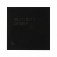
R5S77631Y266BGV Renesas Electronics America, R5S77631Y266BGV Datasheet - Page 1041

R5S77631Y266BGV
Manufacturer Part Number
R5S77631Y266BGV
Description
IC SUPERH MPU ROMLESS 499BGA
Manufacturer
Renesas Electronics America
Series
SuperH® SH7780r
Datasheet
1.R5S77631Y266BGV.pdf
(2056 pages)
Specifications of R5S77631Y266BGV
Core Processor
SH-4A
Core Size
32-Bit
Speed
266MHz
Connectivity
Audio Codec, I²C, MMC, SCI, SIM, SIO, SSI, USB
Peripherals
DMA, LCD, POR, WDT
Number Of I /o
107
Program Memory Type
ROMless
Ram Size
16K x 8
Voltage - Supply (vcc/vdd)
1.15 V ~ 1.35 V
Data Converters
A/D 4x10b; D/A 2x8b
Oscillator Type
External
Operating Temperature
-20°C ~ 75°C
Package / Case
499-BGA
Lead Free Status / RoHS Status
Lead free / RoHS Compliant
Eeprom Size
-
Program Memory Size
-
Available stocks
Company
Part Number
Manufacturer
Quantity
Price
Company:
Part Number:
R5S77631Y266BGV
Manufacturer:
Renesas Electronics America
Quantity:
10 000
- Current page: 1041 of 2056
- Download datasheet (10Mb)
Section 23 Gigabit Ethernet Controller (GETHER)
23.4.5
CAM Function
Frames input to the E-MAC are grouped into the following four types; unicast for this LSI,
broadcast, multicast, and unicast to other destinations. The MAC addresses of unicast for this LSI
and broadcast are fixed, and determined only by register settings. Consequently, only multicast
and unicast to other destinations determine whether to receive or not and whether to transfer or not
by using the CAM (unicast frames whose destination MAC addresses match this LSI are called
unicast frames to this LSI, and those that do not are called unicast frames to other destinations).
Furthermore, the evaluation of receive and relay of unicast to other destinations and multicast
frames by using CAM are performed by referencing the registered MAC addresses of the CAM
entry table in the TSU. By using this function, receive FIFO overflow can be prevented caused by
accumulation of frame data not required for reception, and CPU processing for determining
receive can be reduced.
The POST table is composed of 4 bits, and each bit corresponds to port 0 reception, port 1
reception, port 0 to port 1 relay, and port 1 to port 0 relay. When the corresponding bit is set to 1,
the CAM evaluation results are used for determining receive and relay. In other words, when the
corresponding bit of the POST table is cleared to 0, receive and relay evaluation will be the same
as when CAM is not used shown in table 23.4.
The on-chip CAM has entry tables which can register the MAC address of 32 entries, the details
of which can be set by TSU_ADRH0 to TSU_ADRH31 and TSU_ADRL0 to TSU_ADRL31. The
setting to enable/disable referencing of the on-chip CAM entry table is performed by the CAM
entry table enable setting register which sets whether to perform CAM evaluation or not, and the
CAM entry table POST setting register for setting whether to use the CAM determination results
for determining receive or relay. When on-chip CAM entry table referencing during receive is
enabled, the destination address in the frame and MAC address registered in the CAM entry table
are compared, and it is determined whether to transfer the frames input to the E-MAC to E-DMAC
(have E-DMAC receive the frames) or discard the frames. When relaying and CAM entry table
referencing during relay are both enabled, whether to transfer or discard multicast frames and
frames for destinations other than this LSI can be determined by comparing the destination
address in the frame and MAC address registered in the CAM entry table. Table 23.5 shows the
processing method of frames (receive or discard) in reception from E-MAC0 to E-DMAC0 or that
from E-MAC1 to E-DMAC1, while table 23.6 shows the processing for frames in relay from E-
MAC0 to E-MAC1 or that from E-MAC1 to E-MAC0 (relay or discard).
Rev. 2.00 May 22, 2009 Page 971 of 1982
REJ09B0256-0200
Related parts for R5S77631Y266BGV
Image
Part Number
Description
Manufacturer
Datasheet
Request
R

Part Number:
Description:
KIT STARTER FOR M16C/29
Manufacturer:
Renesas Electronics America
Datasheet:

Part Number:
Description:
KIT STARTER FOR R8C/2D
Manufacturer:
Renesas Electronics America
Datasheet:

Part Number:
Description:
R0K33062P STARTER KIT
Manufacturer:
Renesas Electronics America
Datasheet:

Part Number:
Description:
KIT STARTER FOR R8C/23 E8A
Manufacturer:
Renesas Electronics America
Datasheet:

Part Number:
Description:
KIT STARTER FOR R8C/25
Manufacturer:
Renesas Electronics America
Datasheet:

Part Number:
Description:
KIT STARTER H8S2456 SHARPE DSPLY
Manufacturer:
Renesas Electronics America
Datasheet:

Part Number:
Description:
KIT STARTER FOR R8C38C
Manufacturer:
Renesas Electronics America
Datasheet:

Part Number:
Description:
KIT STARTER FOR R8C35C
Manufacturer:
Renesas Electronics America
Datasheet:

Part Number:
Description:
KIT STARTER FOR R8CL3AC+LCD APPS
Manufacturer:
Renesas Electronics America
Datasheet:

Part Number:
Description:
KIT STARTER FOR RX610
Manufacturer:
Renesas Electronics America
Datasheet:

Part Number:
Description:
KIT STARTER FOR R32C/118
Manufacturer:
Renesas Electronics America
Datasheet:

Part Number:
Description:
KIT DEV RSK-R8C/26-29
Manufacturer:
Renesas Electronics America
Datasheet:

Part Number:
Description:
KIT STARTER FOR SH7124
Manufacturer:
Renesas Electronics America
Datasheet:

Part Number:
Description:
KIT STARTER FOR H8SX/1622
Manufacturer:
Renesas Electronics America
Datasheet:

Part Number:
Description:
KIT DEV FOR SH7203
Manufacturer:
Renesas Electronics America
Datasheet:


