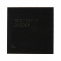
R5S77631Y266BGV Renesas Electronics America, R5S77631Y266BGV Datasheet - Page 446

R5S77631Y266BGV
Manufacturer Part Number
R5S77631Y266BGV
Description
IC SUPERH MPU ROMLESS 499BGA
Manufacturer
Renesas Electronics America
Series
SuperH® SH7780r
Datasheet
1.R5S77631Y266BGV.pdf
(2056 pages)
Specifications of R5S77631Y266BGV
Core Processor
SH-4A
Core Size
32-Bit
Speed
266MHz
Connectivity
Audio Codec, I²C, MMC, SCI, SIM, SIO, SSI, USB
Peripherals
DMA, LCD, POR, WDT
Number Of I /o
107
Program Memory Type
ROMless
Ram Size
16K x 8
Voltage - Supply (vcc/vdd)
1.15 V ~ 1.35 V
Data Converters
A/D 4x10b; D/A 2x8b
Oscillator Type
External
Operating Temperature
-20°C ~ 75°C
Package / Case
499-BGA
Lead Free Status / RoHS Status
Lead free / RoHS Compliant
Eeprom Size
-
Program Memory Size
-
Available stocks
Company
Part Number
Manufacturer
Quantity
Price
Company:
Part Number:
R5S77631Y266BGV
Manufacturer:
Renesas Electronics America
Quantity:
10 000
- Current page: 446 of 2056
- Download datasheet (10Mb)
Section 11 Local Bus State Controller (LBSC)
11.5.5
Areas 5 and 6 can be set to the IC memory card interface or I/O card interface, which is stipulated
in JEIDA specification version 4.2 (PCMCIA 2.1), by setting bits TYPE[2:0] in CS5BCR and
CS6BCR.
Figure 11.15 shows an example of PCMCIA card connection to this LSI. To enable hot insertion
of PCMCIA cards (i.e., insertion or removal while system power is being supplied), a three-state
buffer must be connected between this LSI bus interface and the PCMCIA cards.
Since operation in big-endian mode is not explicitly stipulated in the JEIDA/PCMCIA standard,
this LSI supports the PCMCIA interface only in little-endian mode through little-endian mode
setting.
PCMCIA interface can select space property from among 8-bit common memory, 16-bit common
memory, 8-bit attribute memory, 16-bit attribute memory, 8-bit I/O space, 16-bit I/O space,
dynamic I/O bus sizing, and ATA complement mode by setting bits SAA[2:0] and SAB[2:0] in
CSnPCR.
Rev. 2.00 May 22, 2009 Page 376 of 1982
REJ09B0256-0200
PCMCIA Interface
CLKOUT
A25 to A5
A4 to A0
CSn
RDWR
RD
D31 to D0
(read)
BS
RDY
DACK
Note: * When CSnBCR RDSPL is set to 1.
Figure 11.14 Burst ROM Wait Access Timing
T
AS1
T
1
T
S1
T
B2
T
B1
T
B2
T
B1
T
B2
T
B1
T
2
T
H1
*
T
AH1
Related parts for R5S77631Y266BGV
Image
Part Number
Description
Manufacturer
Datasheet
Request
R

Part Number:
Description:
KIT STARTER FOR M16C/29
Manufacturer:
Renesas Electronics America
Datasheet:

Part Number:
Description:
KIT STARTER FOR R8C/2D
Manufacturer:
Renesas Electronics America
Datasheet:

Part Number:
Description:
R0K33062P STARTER KIT
Manufacturer:
Renesas Electronics America
Datasheet:

Part Number:
Description:
KIT STARTER FOR R8C/23 E8A
Manufacturer:
Renesas Electronics America
Datasheet:

Part Number:
Description:
KIT STARTER FOR R8C/25
Manufacturer:
Renesas Electronics America
Datasheet:

Part Number:
Description:
KIT STARTER H8S2456 SHARPE DSPLY
Manufacturer:
Renesas Electronics America
Datasheet:

Part Number:
Description:
KIT STARTER FOR R8C38C
Manufacturer:
Renesas Electronics America
Datasheet:

Part Number:
Description:
KIT STARTER FOR R8C35C
Manufacturer:
Renesas Electronics America
Datasheet:

Part Number:
Description:
KIT STARTER FOR R8CL3AC+LCD APPS
Manufacturer:
Renesas Electronics America
Datasheet:

Part Number:
Description:
KIT STARTER FOR RX610
Manufacturer:
Renesas Electronics America
Datasheet:

Part Number:
Description:
KIT STARTER FOR R32C/118
Manufacturer:
Renesas Electronics America
Datasheet:

Part Number:
Description:
KIT DEV RSK-R8C/26-29
Manufacturer:
Renesas Electronics America
Datasheet:

Part Number:
Description:
KIT STARTER FOR SH7124
Manufacturer:
Renesas Electronics America
Datasheet:

Part Number:
Description:
KIT STARTER FOR H8SX/1622
Manufacturer:
Renesas Electronics America
Datasheet:

Part Number:
Description:
KIT DEV FOR SH7203
Manufacturer:
Renesas Electronics America
Datasheet:


