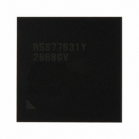
R5S77631Y266BGV Renesas Electronics America, R5S77631Y266BGV Datasheet - Page 56

R5S77631Y266BGV
Manufacturer Part Number
R5S77631Y266BGV
Description
IC SUPERH MPU ROMLESS 499BGA
Manufacturer
Renesas Electronics America
Series
SuperH® SH7780r
Datasheet
1.R5S77631Y266BGV.pdf
(2056 pages)
Specifications of R5S77631Y266BGV
Core Processor
SH-4A
Core Size
32-Bit
Speed
266MHz
Connectivity
Audio Codec, I²C, MMC, SCI, SIM, SIO, SSI, USB
Peripherals
DMA, LCD, POR, WDT
Number Of I /o
107
Program Memory Type
ROMless
Ram Size
16K x 8
Voltage - Supply (vcc/vdd)
1.15 V ~ 1.35 V
Data Converters
A/D 4x10b; D/A 2x8b
Oscillator Type
External
Operating Temperature
-20°C ~ 75°C
Package / Case
499-BGA
Lead Free Status / RoHS Status
Lead free / RoHS Compliant
Eeprom Size
-
Program Memory Size
-
Available stocks
Company
Part Number
Manufacturer
Quantity
Price
Company:
Part Number:
R5S77631Y266BGV
Manufacturer:
Renesas Electronics America
Quantity:
10 000
- Current page: 56 of 2056
- Download datasheet (10Mb)
Figure 38.4 Example of A/D Converter Operation
Figure 38.5 Definitions of A/D Conversion Accuracy ............................................................. 1672
Figure 38.6 Example of Analog Input Pin Protection Circuit................................................... 1673
Section 39 D/A Converter (DAC)
Figure 39.1 Block Diagram of D/A Converter ......................................................................... 1675
Figure 39.2 D/A Converter Operation Example ....................................................................... 1679
Section 41 User Break Controller (UBC)
Figure 41.1 Block Diagram of UBC......................................................................................... 1762
Figure 41.2 Flowchart of User Break Debugging Support Function ........................................ 1792
Section 42 User Debugging Interface (H-UDI)
Figure 42.1 H-UDI Block Diagram .......................................................................................... 1800
Figure 42.2 Sequence for switching from Boundary-Scan TAP Controller to H-UDI............. 1803
Figure 42.3 TAP Controller State Transitions .......................................................................... 1825
Figure 42.4 H-UDI Reset.......................................................................................................... 1826
Section 43 Electrical Characteristics
Figure 43.1 Power-On and Power-Off Timing ......................................................................... 1829
Figure 43.2 EXTAL Clock Input Timing ................................................................................. 1837
Figure 43.3 CLKOUT Clock Output Timing (1)...................................................................... 1837
Figure 43.4 CLKOUT Clock Output Timing (2)...................................................................... 1838
Figure 43.5 Power-On Oscillation Settling Time ..................................................................... 1838
Figure 43.6 PLL Synchronization Settling Time ...................................................................... 1839
Figure 43.7 Oscillation Settling Time on Return from Standby NMI or IRQ .......................... 1839
Figure 43.8 Reset Input Timing................................................................................................ 1839
Figure 43.9 Control Signal Timing........................................................................................... 1840
Figure 43.10 Pin Drive Timing in Standby Mode .................................................................... 1841
Figure 43.11 SRAM Bus Cycle: Basic Bus Cycle (No Wait) .................................................. 1843
Figure 43.12 SRAM Bus Cycle: Basic Bus Cycle (One Wait only by Software) .................... 1844
Figure 43.13 SRAM Bus Cycle: Basic Bus Cycle
Figure 43.14 SRAM Bus Cycle: Basic Bus Cycle
Figure 43.15 Burst ROM Bus Cycle (No Wait) ....................................................................... 1847
Figure 43.16 Burst ROM Bus Cycle
Rev. 2.00 May 22, 2009 Page liv of lxviii
(Scan Mode, Three Channels AN0 to AN2 Selected) ........................................... 1669
(One Wait by Software + One Wait by RDY, RDY Signal is Synchronous
Input) ................................................................................................................... 1845
(No Wait, No Address Setup/Hold Time Insertion, RDS = 1, RDH = 1,
WTS = 1, WTH = 1)............................................................................................ 1846
(1st Data: One Wait by Software + One Wait by RDY;
2nd/3rd/4th Data: One Wait only by software) ................................................... 1848
Related parts for R5S77631Y266BGV
Image
Part Number
Description
Manufacturer
Datasheet
Request
R

Part Number:
Description:
KIT STARTER FOR M16C/29
Manufacturer:
Renesas Electronics America
Datasheet:

Part Number:
Description:
KIT STARTER FOR R8C/2D
Manufacturer:
Renesas Electronics America
Datasheet:

Part Number:
Description:
R0K33062P STARTER KIT
Manufacturer:
Renesas Electronics America
Datasheet:

Part Number:
Description:
KIT STARTER FOR R8C/23 E8A
Manufacturer:
Renesas Electronics America
Datasheet:

Part Number:
Description:
KIT STARTER FOR R8C/25
Manufacturer:
Renesas Electronics America
Datasheet:

Part Number:
Description:
KIT STARTER H8S2456 SHARPE DSPLY
Manufacturer:
Renesas Electronics America
Datasheet:

Part Number:
Description:
KIT STARTER FOR R8C38C
Manufacturer:
Renesas Electronics America
Datasheet:

Part Number:
Description:
KIT STARTER FOR R8C35C
Manufacturer:
Renesas Electronics America
Datasheet:

Part Number:
Description:
KIT STARTER FOR R8CL3AC+LCD APPS
Manufacturer:
Renesas Electronics America
Datasheet:

Part Number:
Description:
KIT STARTER FOR RX610
Manufacturer:
Renesas Electronics America
Datasheet:

Part Number:
Description:
KIT STARTER FOR R32C/118
Manufacturer:
Renesas Electronics America
Datasheet:

Part Number:
Description:
KIT DEV RSK-R8C/26-29
Manufacturer:
Renesas Electronics America
Datasheet:

Part Number:
Description:
KIT STARTER FOR SH7124
Manufacturer:
Renesas Electronics America
Datasheet:

Part Number:
Description:
KIT STARTER FOR H8SX/1622
Manufacturer:
Renesas Electronics America
Datasheet:

Part Number:
Description:
KIT DEV FOR SH7203
Manufacturer:
Renesas Electronics America
Datasheet:


