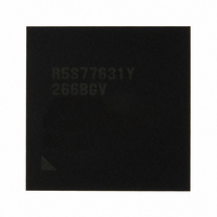
R5S77631Y266BGV Renesas Electronics America, R5S77631Y266BGV Datasheet - Page 252

R5S77631Y266BGV
Manufacturer Part Number
R5S77631Y266BGV
Description
IC SUPERH MPU ROMLESS 499BGA
Manufacturer
Renesas Electronics America
Series
SuperH® SH7780r
Datasheet
1.R5S77631Y266BGV.pdf
(2056 pages)
Specifications of R5S77631Y266BGV
Core Processor
SH-4A
Core Size
32-Bit
Speed
266MHz
Connectivity
Audio Codec, I²C, MMC, SCI, SIM, SIO, SSI, USB
Peripherals
DMA, LCD, POR, WDT
Number Of I /o
107
Program Memory Type
ROMless
Ram Size
16K x 8
Voltage - Supply (vcc/vdd)
1.15 V ~ 1.35 V
Data Converters
A/D 4x10b; D/A 2x8b
Oscillator Type
External
Operating Temperature
-20°C ~ 75°C
Package / Case
499-BGA
Lead Free Status / RoHS Status
Lead free / RoHS Compliant
Eeprom Size
-
Program Memory Size
-
Available stocks
Company
Part Number
Manufacturer
Quantity
Price
Company:
Part Number:
R5S77631Y266BGV
Manufacturer:
Renesas Electronics America
Quantity:
10 000
- Current page: 252 of 2056
- Download datasheet (10Mb)
Section 6 Memory Management Unit (MMU)
6.7.5
To enable the PMB to be managed by software, its contents are allowed to be read from and
written to by a P1 or P2 area program with a MOV instruction in privileged mode. The PMB
address array is allocated to addresses H'F610 0000 to H'F61F FFFF in the P4 area and the PMB
data array to addresses H'F710 0000 to H'F71F FFFF in the P4 area. VPN and V in the PMB can
be accessed as an address array, PPN, V, SZ, C, WT, and UB as a data array. V can be accessed
from both the address array side and the data array side. A program which executes a PMB
memory-mapped access should be placed in the page area at which the C bit in PMB is cleared to
0.
1. PMB address array read
2. PMB address array write
3. PMB data array read
4. PMB data array write
Rev. 2.00 May 22, 2009 Page 182 of 1982
REJ09B0256-0200
When memory reading is performed while bits 31 to 20 in the address field are specified as
H'F61 which indicates the PMB address array and bits 11 to 8 in the address field as an entry,
bits 31 to 24 in the data field are read as VPN and bit 8 in the data field as V.
When memory writing is performed while bits 31 to 20 in the address field are specified as
H'F61 which indicates the PMB address array and bits 11 to 8 in the address field as an entry,
and bits 31 to 24 in the data field are specified as VPN and bit 8 in the data field as V, data is
written to the specified entry.
When memory reading is performed while bits 31 to 20 in the address field are specified as
H'F71 which indicates the PMB data array and bits 11 to 8 in the address field as an entry, bits
31 to 24 in the data field are read as PPN, bit 9 in the data field as UB, bit 8 in the data field as
V, bits 7 and 4 in the data field as SZ, bit 3 in the data field as C, and bit 0 in the data field as
WT.
When memory writing is performed while bits 31 to 20 in the address field are specified as
H'F71 which indicates the PMB data array and bits 11 to 8 in the address field as an entry, and
bits 31 to 24 in the data field are specified as PPN, bit 9 in the data field as UB, bit 8 in the
data field as V, bits 7 and 4 in the data field as SZ, bit 3 in the data field as C, and bit 0 in the
data field as WT, data is written to the specified entry.
Memory-Mapped PMB Configuration
Related parts for R5S77631Y266BGV
Image
Part Number
Description
Manufacturer
Datasheet
Request
R

Part Number:
Description:
KIT STARTER FOR M16C/29
Manufacturer:
Renesas Electronics America
Datasheet:

Part Number:
Description:
KIT STARTER FOR R8C/2D
Manufacturer:
Renesas Electronics America
Datasheet:

Part Number:
Description:
R0K33062P STARTER KIT
Manufacturer:
Renesas Electronics America
Datasheet:

Part Number:
Description:
KIT STARTER FOR R8C/23 E8A
Manufacturer:
Renesas Electronics America
Datasheet:

Part Number:
Description:
KIT STARTER FOR R8C/25
Manufacturer:
Renesas Electronics America
Datasheet:

Part Number:
Description:
KIT STARTER H8S2456 SHARPE DSPLY
Manufacturer:
Renesas Electronics America
Datasheet:

Part Number:
Description:
KIT STARTER FOR R8C38C
Manufacturer:
Renesas Electronics America
Datasheet:

Part Number:
Description:
KIT STARTER FOR R8C35C
Manufacturer:
Renesas Electronics America
Datasheet:

Part Number:
Description:
KIT STARTER FOR R8CL3AC+LCD APPS
Manufacturer:
Renesas Electronics America
Datasheet:

Part Number:
Description:
KIT STARTER FOR RX610
Manufacturer:
Renesas Electronics America
Datasheet:

Part Number:
Description:
KIT STARTER FOR R32C/118
Manufacturer:
Renesas Electronics America
Datasheet:

Part Number:
Description:
KIT DEV RSK-R8C/26-29
Manufacturer:
Renesas Electronics America
Datasheet:

Part Number:
Description:
KIT STARTER FOR SH7124
Manufacturer:
Renesas Electronics America
Datasheet:

Part Number:
Description:
KIT STARTER FOR H8SX/1622
Manufacturer:
Renesas Electronics America
Datasheet:

Part Number:
Description:
KIT DEV FOR SH7203
Manufacturer:
Renesas Electronics America
Datasheet:


