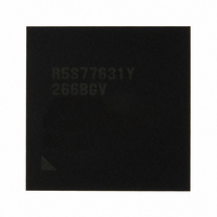
R5S77631Y266BGV Renesas Electronics America, R5S77631Y266BGV Datasheet - Page 1353

R5S77631Y266BGV
Manufacturer Part Number
R5S77631Y266BGV
Description
IC SUPERH MPU ROMLESS 499BGA
Manufacturer
Renesas Electronics America
Series
SuperH® SH7780r
Datasheet
1.R5S77631Y266BGV.pdf
(2056 pages)
Specifications of R5S77631Y266BGV
Core Processor
SH-4A
Core Size
32-Bit
Speed
266MHz
Connectivity
Audio Codec, I²C, MMC, SCI, SIM, SIO, SSI, USB
Peripherals
DMA, LCD, POR, WDT
Number Of I /o
107
Program Memory Type
ROMless
Ram Size
16K x 8
Voltage - Supply (vcc/vdd)
1.15 V ~ 1.35 V
Data Converters
A/D 4x10b; D/A 2x8b
Oscillator Type
External
Operating Temperature
-20°C ~ 75°C
Package / Case
499-BGA
Lead Free Status / RoHS Status
Lead free / RoHS Compliant
Eeprom Size
-
Program Memory Size
-
Available stocks
Company
Part Number
Manufacturer
Quantity
Price
Company:
Part Number:
R5S77631Y266BGV
Manufacturer:
Renesas Electronics America
Quantity:
10 000
- Current page: 1353 of 2056
- Download datasheet (10Mb)
(3)
When switching between smart card interface mode and standby mode, in order to retain the clock
duty, the following switching procedure should be used. Step (1) to step (7) of figure 30.10
correspond to the following operation.
• When switching from smart card interface mode to standby mode
1. Write 0 to the TE and RE bits in the serial control register (SCSCR), to stop transmit and
2. Write 0 to the CKE0 bit in SCSCR to stop the clock.
3. Wait for one cycle of the serial clock. During this interval, the duty is retained, and the clock
4. Make the transition to standby mode.
• To return from standby mode to smart card interface mode
5. Cancel the standby state.
6. Set the CKE1 bit in the serial control register (SCSCR) to the value of the output-fixed state at
7. Write 1 to the CKE0 bit in SCSCR to output a clock signal. Clock signal generation begins at
(4)
In order to retain the clock duty from power-on, the following switching procedure should be
used.
1. The initial state is set to port-input with high impedance. In order to fix the potential, a pull-up
2. Use the CKE1 bit in the serial control register (SCSCR) to fix the specified output.
3. Set the CKE0 bit in SCSCR to 1 to start clock output.
receive operations. At the same time, set the CKE1 bit to the value for the output-fixed state in
standby mode.
output is fixed at the specified level.
the beginning of standby (the current SIM_CLK pin state).
normal duty.
resistance/pull-down resistance is used.
Standby Mode Switching
Power-On and Clock Output
SIM_CLK
Figure 30.10 Procedure for Stopping Clock and Restarting
(1) (2) (3)
Normal operation
(4)
Standby mode
(5) (6) (7)
Rev. 2.00 May 22, 2009 Page 1283 of 1982
Section 30 SIM Card Module (SIM)
Normal operation
REJ09B0256-0200
Related parts for R5S77631Y266BGV
Image
Part Number
Description
Manufacturer
Datasheet
Request
R

Part Number:
Description:
KIT STARTER FOR M16C/29
Manufacturer:
Renesas Electronics America
Datasheet:

Part Number:
Description:
KIT STARTER FOR R8C/2D
Manufacturer:
Renesas Electronics America
Datasheet:

Part Number:
Description:
R0K33062P STARTER KIT
Manufacturer:
Renesas Electronics America
Datasheet:

Part Number:
Description:
KIT STARTER FOR R8C/23 E8A
Manufacturer:
Renesas Electronics America
Datasheet:

Part Number:
Description:
KIT STARTER FOR R8C/25
Manufacturer:
Renesas Electronics America
Datasheet:

Part Number:
Description:
KIT STARTER H8S2456 SHARPE DSPLY
Manufacturer:
Renesas Electronics America
Datasheet:

Part Number:
Description:
KIT STARTER FOR R8C38C
Manufacturer:
Renesas Electronics America
Datasheet:

Part Number:
Description:
KIT STARTER FOR R8C35C
Manufacturer:
Renesas Electronics America
Datasheet:

Part Number:
Description:
KIT STARTER FOR R8CL3AC+LCD APPS
Manufacturer:
Renesas Electronics America
Datasheet:

Part Number:
Description:
KIT STARTER FOR RX610
Manufacturer:
Renesas Electronics America
Datasheet:

Part Number:
Description:
KIT STARTER FOR R32C/118
Manufacturer:
Renesas Electronics America
Datasheet:

Part Number:
Description:
KIT DEV RSK-R8C/26-29
Manufacturer:
Renesas Electronics America
Datasheet:

Part Number:
Description:
KIT STARTER FOR SH7124
Manufacturer:
Renesas Electronics America
Datasheet:

Part Number:
Description:
KIT STARTER FOR H8SX/1622
Manufacturer:
Renesas Electronics America
Datasheet:

Part Number:
Description:
KIT DEV FOR SH7203
Manufacturer:
Renesas Electronics America
Datasheet:


