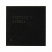
R5S77631Y266BGV Renesas Electronics America, R5S77631Y266BGV Datasheet - Page 204

R5S77631Y266BGV
Manufacturer Part Number
R5S77631Y266BGV
Description
IC SUPERH MPU ROMLESS 499BGA
Manufacturer
Renesas Electronics America
Series
SuperH® SH7780r
Datasheet
1.R5S77631Y266BGV.pdf
(2056 pages)
Specifications of R5S77631Y266BGV
Core Processor
SH-4A
Core Size
32-Bit
Speed
266MHz
Connectivity
Audio Codec, I²C, MMC, SCI, SIM, SIO, SSI, USB
Peripherals
DMA, LCD, POR, WDT
Number Of I /o
107
Program Memory Type
ROMless
Ram Size
16K x 8
Voltage - Supply (vcc/vdd)
1.15 V ~ 1.35 V
Data Converters
A/D 4x10b; D/A 2x8b
Oscillator Type
External
Operating Temperature
-20°C ~ 75°C
Package / Case
499-BGA
Lead Free Status / RoHS Status
Lead free / RoHS Compliant
Eeprom Size
-
Program Memory Size
-
Available stocks
Company
Part Number
Manufacturer
Quantity
Price
Company:
Part Number:
R5S77631Y266BGV
Manufacturer:
Renesas Electronics America
Quantity:
10 000
- Current page: 204 of 2056
- Download datasheet (10Mb)
Section 5 Exception Handling
• Indivisible delayed branch instruction and delay slot instruction
Rev. 2.00 May 22, 2009 Page 134 of 1982
REJ09B0256-0200
With MAC instructions, memory-to-memory arithmetic/logic instructions, TAS instructions,
and MOVUA instructions, two data transfers are performed by a single instruction, and an
exception will be detected for each of these data transfers. In these cases, therefore, the
following order is used to determine priority.
1. Data address error in first data transfer
2. TLB miss in first data transfer
3. TLB protection violation in first data transfer
4. Initial page write exception in first data transfer
5. Data address error in second data transfer
6. TLB miss in second data transfer
7. TLB protection violation in second data transfer
8. Initial page write exception in second data transfer
As a delayed branch instruction and its associated delay slot instruction are indivisible, they
are treated as a single instruction. Consequently, the priority order for exceptions that occur in
these instructions differs from the usual priority order. The priority order shown below is for
the case where the delay slot instruction has only one data transfer.
1. A check is performed for the interrupt type and re-execution type exceptions of priority
2. A check is performed for the interrupt type and re-execution type exceptions of priority
3. A check is performed for the completion type exception of priority level 2 in the delayed
4. A check is performed for the completion type exception of priority level 2 in the delay slot
5. A check is performed for priority level 3 in the delayed branch instruction and priority
6. A check is performed for priority level 4 in the delayed branch instruction and priority
If the delay slot instruction has a second data transfer, two checks are performed in step 2, as in
the above case (Instructions that make two accesses to memory).
If the accepted exception (the highest-priority exception) is a delay slot instruction re-
execution type exception, the branch instruction PR register write operation (PC → PR
operation performed in a BSR, BSRF, or JSR instruction) is not disabled. Note that in this
case, the contents of PR register are not guaranteed.
levels 1 and 2 in the delayed branch instruction.
levels 1 and 2 in the delay slot instruction.
branch instruction.
instruction.
level 3 in the delay slot instruction. (There is no priority ranking between these two.)
level 4 in the delay slot instruction. (There is no priority ranking between these two.)
Related parts for R5S77631Y266BGV
Image
Part Number
Description
Manufacturer
Datasheet
Request
R

Part Number:
Description:
KIT STARTER FOR M16C/29
Manufacturer:
Renesas Electronics America
Datasheet:

Part Number:
Description:
KIT STARTER FOR R8C/2D
Manufacturer:
Renesas Electronics America
Datasheet:

Part Number:
Description:
R0K33062P STARTER KIT
Manufacturer:
Renesas Electronics America
Datasheet:

Part Number:
Description:
KIT STARTER FOR R8C/23 E8A
Manufacturer:
Renesas Electronics America
Datasheet:

Part Number:
Description:
KIT STARTER FOR R8C/25
Manufacturer:
Renesas Electronics America
Datasheet:

Part Number:
Description:
KIT STARTER H8S2456 SHARPE DSPLY
Manufacturer:
Renesas Electronics America
Datasheet:

Part Number:
Description:
KIT STARTER FOR R8C38C
Manufacturer:
Renesas Electronics America
Datasheet:

Part Number:
Description:
KIT STARTER FOR R8C35C
Manufacturer:
Renesas Electronics America
Datasheet:

Part Number:
Description:
KIT STARTER FOR R8CL3AC+LCD APPS
Manufacturer:
Renesas Electronics America
Datasheet:

Part Number:
Description:
KIT STARTER FOR RX610
Manufacturer:
Renesas Electronics America
Datasheet:

Part Number:
Description:
KIT STARTER FOR R32C/118
Manufacturer:
Renesas Electronics America
Datasheet:

Part Number:
Description:
KIT DEV RSK-R8C/26-29
Manufacturer:
Renesas Electronics America
Datasheet:

Part Number:
Description:
KIT STARTER FOR SH7124
Manufacturer:
Renesas Electronics America
Datasheet:

Part Number:
Description:
KIT STARTER FOR H8SX/1622
Manufacturer:
Renesas Electronics America
Datasheet:

Part Number:
Description:
KIT DEV FOR SH7203
Manufacturer:
Renesas Electronics America
Datasheet:


