R5S77631Y266BGV Renesas Electronics America, R5S77631Y266BGV Datasheet - Page 64
R5S77631Y266BGV
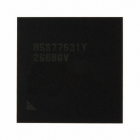
Manufacturer Part Number
R5S77631Y266BGV
Description
IC SUPERH MPU ROMLESS 499BGA
Manufacturer
Renesas Electronics America
Series
SuperH® SH7780r
Datasheet
1.R5S77631Y266BGV.pdf
(2056 pages)
Specifications of R5S77631Y266BGV
Core Processor
SH-4A
Core Size
32-Bit
Speed
266MHz
Connectivity
Audio Codec, I²C, MMC, SCI, SIM, SIO, SSI, USB
Peripherals
DMA, LCD, POR, WDT
Number Of I /o
107
Program Memory Type
ROMless
Ram Size
16K x 8
Voltage - Supply (vcc/vdd)
1.15 V ~ 1.35 V
Data Converters
A/D 4x10b; D/A 2x8b
Oscillator Type
External
Operating Temperature
-20°C ~ 75°C
Package / Case
499-BGA
Lead Free Status / RoHS Status
Lead free / RoHS Compliant
Eeprom Size
-
Program Memory Size
-
Available stocks
Company
Part Number
Manufacturer
Quantity
Price
Company:

Part Number:
R5S77631Y266BGV
Manufacturer:
Renesas Electronics America
Quantity:
10 000


Table 15.4
Table 15.5
Section 16 Clock Pulse Generator (CPG)
Table 16.1
Table 16.2
Table 16.3
Table 16.4
Section 17 Watchdog Timer and Reset (WDT)
Table 17.1
Table 17.2
Table 17.3
Section 18 Power-Down Mode
Table 18.1
Table 18.2
Table 18.3
Table 18.4
Table 18.5
Section 19 Timer Unit (TMU)
Table 19.1
Table 19.2
Table 19.3
Table 19.4
Section 20 16-Bit Timer Pulse Unit (TPU)
Table 20.1
Table 20.2
Table 20.3
Table 20.4
Table 20.5
Table 20.6
Table 20.6
Table 20.6
Table 20.6
Table 20.7
Table 20.8
Table 20.9
Table 20.10
Table 20.11
Table 20.12
Rev. 2.00 May 22, 2009 Page lxii of lxviii
Access and Data Alignment for Little Endian ...................................................... 630
Access and Data Alignment for Big Endian ......................................................... 631
Pin Configuration and Functions of CPG ............................................................. 638
Clock Operating Modes ........................................................................................ 639
Register Configuration.......................................................................................... 640
Register States in Each Operating Mode .............................................................. 640
Pin Configuration.................................................................................................. 649
Register Configuration.......................................................................................... 650
Register State in Each Operating Mode................................................................ 650
States in Power-Down Modes............................................................................... 670
Pin Configuration.................................................................................................. 671
Register Configuration.......................................................................................... 672
Register States in Each Operating Mode .............................................................. 672
Pin Configuration.................................................................................................. 686
Pin Configuration.................................................................................................. 691
Register Configuration.......................................................................................... 692
Register States in Each Operating Mode .............................................................. 693
TMU Interrupt Sources......................................................................................... 706
TPU Functions ...................................................................................................... 710
TPU Pin Configurations........................................................................................ 712
Register Configuration.......................................................................................... 713
Register State in Each Operating Mode................................................................ 715
TPU Clock Sources............................................................................................... 718
TPSC[2:0] (1) ....................................................................................................... 719
TPSC[2:0] (2) ....................................................................................................... 719
TPSC[2:0] (3) ....................................................................................................... 719
TPSC[2:0] (4) ....................................................................................................... 720
IOA[2:0] ............................................................................................................... 724
Register Combinations in Buffer Operation ......................................................... 736
Phase Counting Mode Clock Input Pins ............................................................... 742
Up/Down-Count Conditions in Phase Counting Mode 1.................................. 744
Up/Down-Count Conditions in Phase Counting Mode 2.................................. 745
Up/Down-Count Conditions in Phase Counting Mode 3.................................. 746
Related parts for R5S77631Y266BGV
Image
Part Number
Description
Manufacturer
Datasheet
Request
R

Part Number:
Description:
KIT STARTER FOR M16C/29
Manufacturer:
Renesas Electronics America
Datasheet:

Part Number:
Description:
KIT STARTER FOR R8C/2D
Manufacturer:
Renesas Electronics America
Datasheet:

Part Number:
Description:
R0K33062P STARTER KIT
Manufacturer:
Renesas Electronics America
Datasheet:

Part Number:
Description:
KIT STARTER FOR R8C/23 E8A
Manufacturer:
Renesas Electronics America
Datasheet:

Part Number:
Description:
KIT STARTER FOR R8C/25
Manufacturer:
Renesas Electronics America
Datasheet:

Part Number:
Description:
KIT STARTER H8S2456 SHARPE DSPLY
Manufacturer:
Renesas Electronics America
Datasheet:

Part Number:
Description:
KIT STARTER FOR R8C38C
Manufacturer:
Renesas Electronics America
Datasheet:

Part Number:
Description:
KIT STARTER FOR R8C35C
Manufacturer:
Renesas Electronics America
Datasheet:

Part Number:
Description:
KIT STARTER FOR R8CL3AC+LCD APPS
Manufacturer:
Renesas Electronics America
Datasheet:
Part Number:
Description:
KIT STARTER FOR RX610
Manufacturer:
Renesas Electronics America
Datasheet:

Part Number:
Description:
KIT STARTER FOR R32C/118
Manufacturer:
Renesas Electronics America
Datasheet:

Part Number:
Description:
KIT DEV RSK-R8C/26-29
Manufacturer:
Renesas Electronics America
Datasheet:

Part Number:
Description:
KIT STARTER FOR SH7124
Manufacturer:
Renesas Electronics America
Datasheet:

Part Number:
Description:
KIT STARTER FOR H8SX/1622
Manufacturer:
Renesas Electronics America
Datasheet:

Part Number:
Description:
KIT DEV FOR SH7203
Manufacturer:
Renesas Electronics America
Datasheet: