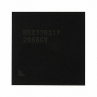
R5S77631Y266BGV Renesas Electronics America, R5S77631Y266BGV Datasheet - Page 223

R5S77631Y266BGV
Manufacturer Part Number
R5S77631Y266BGV
Description
IC SUPERH MPU ROMLESS 499BGA
Manufacturer
Renesas Electronics America
Series
SuperH® SH7780r
Datasheet
1.R5S77631Y266BGV.pdf
(2056 pages)
Specifications of R5S77631Y266BGV
Core Processor
SH-4A
Core Size
32-Bit
Speed
266MHz
Connectivity
Audio Codec, I²C, MMC, SCI, SIM, SIO, SSI, USB
Peripherals
DMA, LCD, POR, WDT
Number Of I /o
107
Program Memory Type
ROMless
Ram Size
16K x 8
Voltage - Supply (vcc/vdd)
1.15 V ~ 1.35 V
Data Converters
A/D 4x10b; D/A 2x8b
Oscillator Type
External
Operating Temperature
-20°C ~ 75°C
Package / Case
499-BGA
Lead Free Status / RoHS Status
Lead free / RoHS Compliant
Eeprom Size
-
Program Memory Size
-
Available stocks
Company
Part Number
Manufacturer
Quantity
Price
Company:
Part Number:
R5S77631Y266BGV
Manufacturer:
Renesas Electronics America
Quantity:
10 000
- Current page: 223 of 2056
- Download datasheet (10Mb)
6.2.7
When the specific resource is changed, IRMCR controls whether the instruction fetch is
performed again for the next instruction. The specific resource means the part of control registers,
TLB, and cache.
In the initial state, the instruction fetch is performed again for the next instruction after changing
the resource. However, the CPU processing performance will be lowered because the instruction
fetch is performed again for the next instruction every time the resource is changed. Therefore, it
is recommended that each bit in IRMCR is set to 1 and the specific instruction should be executed
after all necessary resources have been changed prior to execution of the program which uses
changed resources.
For details on the specific sequence, see descriptions in each resource.
Bit
7 to 0
Instruction Re-Fetch Inhibit Control Register (IRMCR)
Bit Name
UB
Initial
Value
All 0
R/W
R/W
Description
Buffered Write Control for Each Area (64 Mbytes)
When writing is performed without using the cache or in
the cache write-through mode, these bits specify
whether the next bus access from the CPU waits for the
end of writing for each area.
0: The CPU does not wait for the end of writing bus
1: The CPU waits for the end of writing bus access and
UB[7]: Corresponding to the control register area
UB[6]: Corresponding to area 6
UB[5]: Corresponding to area 5
UB[4]: Corresponding to area 4
UB[3]: Corresponding to area 3
UB[2]: Corresponding to area 2
UB[1]: Corresponding to area 1
UB[0]: Corresponding to area 0
access and starts the next bus access
starts the next bus access
Section 6 Memory Management Unit (MMU)
Rev. 2.00 May 22, 2009 Page 153 of 1982
REJ09B0256-0200
Related parts for R5S77631Y266BGV
Image
Part Number
Description
Manufacturer
Datasheet
Request
R

Part Number:
Description:
KIT STARTER FOR M16C/29
Manufacturer:
Renesas Electronics America
Datasheet:

Part Number:
Description:
KIT STARTER FOR R8C/2D
Manufacturer:
Renesas Electronics America
Datasheet:

Part Number:
Description:
R0K33062P STARTER KIT
Manufacturer:
Renesas Electronics America
Datasheet:

Part Number:
Description:
KIT STARTER FOR R8C/23 E8A
Manufacturer:
Renesas Electronics America
Datasheet:

Part Number:
Description:
KIT STARTER FOR R8C/25
Manufacturer:
Renesas Electronics America
Datasheet:

Part Number:
Description:
KIT STARTER H8S2456 SHARPE DSPLY
Manufacturer:
Renesas Electronics America
Datasheet:

Part Number:
Description:
KIT STARTER FOR R8C38C
Manufacturer:
Renesas Electronics America
Datasheet:

Part Number:
Description:
KIT STARTER FOR R8C35C
Manufacturer:
Renesas Electronics America
Datasheet:

Part Number:
Description:
KIT STARTER FOR R8CL3AC+LCD APPS
Manufacturer:
Renesas Electronics America
Datasheet:

Part Number:
Description:
KIT STARTER FOR RX610
Manufacturer:
Renesas Electronics America
Datasheet:

Part Number:
Description:
KIT STARTER FOR R32C/118
Manufacturer:
Renesas Electronics America
Datasheet:

Part Number:
Description:
KIT DEV RSK-R8C/26-29
Manufacturer:
Renesas Electronics America
Datasheet:

Part Number:
Description:
KIT STARTER FOR SH7124
Manufacturer:
Renesas Electronics America
Datasheet:

Part Number:
Description:
KIT STARTER FOR H8SX/1622
Manufacturer:
Renesas Electronics America
Datasheet:

Part Number:
Description:
KIT DEV FOR SH7203
Manufacturer:
Renesas Electronics America
Datasheet:


