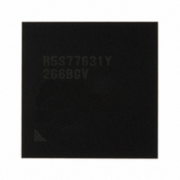
R5S77631Y266BGV Renesas Electronics America, R5S77631Y266BGV Datasheet - Page 53

R5S77631Y266BGV
Manufacturer Part Number
R5S77631Y266BGV
Description
IC SUPERH MPU ROMLESS 499BGA
Manufacturer
Renesas Electronics America
Series
SuperH® SH7780r
Datasheet
1.R5S77631Y266BGV.pdf
(2056 pages)
Specifications of R5S77631Y266BGV
Core Processor
SH-4A
Core Size
32-Bit
Speed
266MHz
Connectivity
Audio Codec, I²C, MMC, SCI, SIM, SIO, SSI, USB
Peripherals
DMA, LCD, POR, WDT
Number Of I /o
107
Program Memory Type
ROMless
Ram Size
16K x 8
Voltage - Supply (vcc/vdd)
1.15 V ~ 1.35 V
Data Converters
A/D 4x10b; D/A 2x8b
Oscillator Type
External
Operating Temperature
-20°C ~ 75°C
Package / Case
499-BGA
Lead Free Status / RoHS Status
Lead free / RoHS Compliant
Eeprom Size
-
Program Memory Size
-
Available stocks
Company
Part Number
Manufacturer
Quantity
Price
Company:
Part Number:
R5S77631Y266BGV
Manufacturer:
Renesas Electronics America
Quantity:
10 000
- Current page: 53 of 2056
- Download datasheet (10Mb)
Figure 31.18 (1) Example of Operational Flow for Commands with Write Data
Figure 31.18 (2) Example of Operational Flow for Commands with Write Data
Figure 31.19 (1) Example of Operational Flow for Auto-mode Pre-defined Multiblock
Figure 31.19 (2) Example of Operational Flow for Auto-mode Pre-defined Multiblock
Figure 31.20 (1) Example of Operational Flow for Auto-mode Pre-defined Multiblock
Figure 31.20 (2) Example of Operational Flow for Auto-mode Pre-defined Multiblock
Figure 31.21 Operation Flow to Apply the Card Identification Function................................. 1360
Section 32 PC Card Controller (PCC)
Figure 32.1 PC Card Controller Block Diagram....................................................................... 1362
Figure 32.2 Continuous 32-Mbyte Area Mode......................................................................... 1364
Figure 32.3 Continuous 16-Mbyte Area Mode (Area 6)........................................................... 1365
Figure 32.4 SH7763 Interface................................................................................................... 1382
Figure 32.5 PCMCIA Memory Card Interface Basic Timing................................................... 1386
Figure 32.6 PCMCIA Memory Card Interface Wait Timing.................................................... 1387
Figure 32.7 PCMCIA I/O Card Interface Basic Timing ........................................................... 1388
Figure 32.8 PCMCIA I/O Card Interface Wait Timing ............................................................ 1389
Figure 32.9 Dynamic Bus Sizing Timing for PCMCIA I/O Card Interface ............................. 1390
Section 33 Audio Codec Interface (HAC)
Figure 33.1 Block Diagram ...................................................................................................... 1394
Figure 33.2 AC97 Frame Slot Structure ................................................................................... 1411
Figure 33.3 Initialization Sequence .......................................................................................... 1414
Figure 33.4 Sample Flowchart for Off-Chip Codec Register Write ......................................... 1415
Figure 33.5 Sample Flowchart for Off-Chip Codec Register Read (1) .................................... 1416
Figure 33.6 Sample Flowchart for Off-Chip Codec Register Read (2) .................................... 1417
Figure 33.7 Sample Flowchart for Off-Chip Codec Register Read (3) .................................... 1418
Section 34 Serial Sound Interface (SSI)
Figure 34.1 Block Diagram of SSI Module .............................................................................. 1422
Figure 34.2 Philips Format (with no Padding).......................................................................... 1441
Figure 34.3 Philips Format (with Padding)............................................................................... 1441
Figure 34.4 Sony Format (with Serial Data First, Followed by Padding Bits) ......................... 1442
Figure 34.5 Matsushita Format (with Padding Bits First, Followed by Serial Data)................ 1442
Figure 34.6 Multichannel Format (2 Channels, No Padding)................................................... 1444
Figure 34.7 Multichannel Format (3 Channels with High Padding)......................................... 1444
(Pre-defined Multiblock Transfer)................................................................. 1351
(Pre-defined Multiblock Transfer)................................................................. 1352
Read Transfer................................................................................................. 1354
Read Transfer................................................................................................. 1355
Write Transfer................................................................................................ 1357
Write Transfer................................................................................................ 1358
Rev. 2.00 May 22, 2009 Page li of lxviii
Related parts for R5S77631Y266BGV
Image
Part Number
Description
Manufacturer
Datasheet
Request
R

Part Number:
Description:
KIT STARTER FOR M16C/29
Manufacturer:
Renesas Electronics America
Datasheet:

Part Number:
Description:
KIT STARTER FOR R8C/2D
Manufacturer:
Renesas Electronics America
Datasheet:

Part Number:
Description:
R0K33062P STARTER KIT
Manufacturer:
Renesas Electronics America
Datasheet:

Part Number:
Description:
KIT STARTER FOR R8C/23 E8A
Manufacturer:
Renesas Electronics America
Datasheet:

Part Number:
Description:
KIT STARTER FOR R8C/25
Manufacturer:
Renesas Electronics America
Datasheet:

Part Number:
Description:
KIT STARTER H8S2456 SHARPE DSPLY
Manufacturer:
Renesas Electronics America
Datasheet:

Part Number:
Description:
KIT STARTER FOR R8C38C
Manufacturer:
Renesas Electronics America
Datasheet:

Part Number:
Description:
KIT STARTER FOR R8C35C
Manufacturer:
Renesas Electronics America
Datasheet:

Part Number:
Description:
KIT STARTER FOR R8CL3AC+LCD APPS
Manufacturer:
Renesas Electronics America
Datasheet:

Part Number:
Description:
KIT STARTER FOR RX610
Manufacturer:
Renesas Electronics America
Datasheet:

Part Number:
Description:
KIT STARTER FOR R32C/118
Manufacturer:
Renesas Electronics America
Datasheet:

Part Number:
Description:
KIT DEV RSK-R8C/26-29
Manufacturer:
Renesas Electronics America
Datasheet:

Part Number:
Description:
KIT STARTER FOR SH7124
Manufacturer:
Renesas Electronics America
Datasheet:

Part Number:
Description:
KIT STARTER FOR H8SX/1622
Manufacturer:
Renesas Electronics America
Datasheet:

Part Number:
Description:
KIT DEV FOR SH7203
Manufacturer:
Renesas Electronics America
Datasheet:


