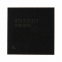
R5S77631Y266BGV Renesas Electronics America, R5S77631Y266BGV Datasheet - Page 1688

R5S77631Y266BGV
Manufacturer Part Number
R5S77631Y266BGV
Description
IC SUPERH MPU ROMLESS 499BGA
Manufacturer
Renesas Electronics America
Series
SuperH® SH7780r
Datasheet
1.R5S77631Y266BGV.pdf
(2056 pages)
Specifications of R5S77631Y266BGV
Core Processor
SH-4A
Core Size
32-Bit
Speed
266MHz
Connectivity
Audio Codec, I²C, MMC, SCI, SIM, SIO, SSI, USB
Peripherals
DMA, LCD, POR, WDT
Number Of I /o
107
Program Memory Type
ROMless
Ram Size
16K x 8
Voltage - Supply (vcc/vdd)
1.15 V ~ 1.35 V
Data Converters
A/D 4x10b; D/A 2x8b
Oscillator Type
External
Operating Temperature
-20°C ~ 75°C
Package / Case
499-BGA
Lead Free Status / RoHS Status
Lead free / RoHS Compliant
Eeprom Size
-
Program Memory Size
-
Available stocks
Company
Part Number
Manufacturer
Quantity
Price
Company:
Part Number:
R5S77631Y266BGV
Manufacturer:
Renesas Electronics America
Quantity:
10 000
- Current page: 1688 of 2056
- Download datasheet (10Mb)
Section 37 LCD Controller (LCDC)
37.3.18 LCDC Power-Supply Sequence Period Register (LDPSPR)
LDPSPR controls the power supply circuit that provides power to the LCD module. The timing to
start outputting the timing signals to the LCD_VEPWC and LCD_VCPWC pins is specified.
Rev. 2.00 May 22, 2009 Page 1618 of 1982
REJ09B0256-0200
Initial value:
Bit
15 to 12 ONA[3:0]
11 to 8
R/W:
Bit:
R/W
Bit Name
ONB[3:0]
15
1
R/W
14
1
ONA[3:0]
R/W
13
1
Initial Value R/W
1111
0110
R/W
12
1
R/W
11
0
R/W
10
R/W
R/W
1
ONB[3:0]
R/W
9
1
LCDC Power-On Sequence Period
LCDC Power-On Sequence Period
Description
Set the period from LCD_VCPWC assertion to
starting output of the display data (LCD_D) and
timing signals (LCD_FLM, LCD_CL1, LCD_CL2,
and LCD_M_DISP) in the power-on sequence of the
LCD module in frame units.
Specify to the value of (the period)-1.
This period is the (a) period in figures 37.4 to 37.7,
Power-Supply Control Sequence and States of the
LCD Module.
Set the period from starting output of the display
data (LCD_D) and timing signals (LCD_FLM,
LCD_CL1, LCD_CL2, and LCD_M_DISP) to the
LCD_VEPWC assertion in the power-on sequence
of the LCD module in frame units.
Specify to the value of (the period)-1.
This period is the (b) period in figures 37.4 to 37.7,
Power-Supply Control Sequence and States of the
LCD Module.
R/W
8
0
R/W
7
0
R/W
OFFE[3:0]
6
0
R/W
5
0
R/W
4
0
R/W
3
1
R/W
2
OFFF[3:0]
1
R/W
1
1
R/W
0
1
Related parts for R5S77631Y266BGV
Image
Part Number
Description
Manufacturer
Datasheet
Request
R

Part Number:
Description:
KIT STARTER FOR M16C/29
Manufacturer:
Renesas Electronics America
Datasheet:

Part Number:
Description:
KIT STARTER FOR R8C/2D
Manufacturer:
Renesas Electronics America
Datasheet:

Part Number:
Description:
R0K33062P STARTER KIT
Manufacturer:
Renesas Electronics America
Datasheet:

Part Number:
Description:
KIT STARTER FOR R8C/23 E8A
Manufacturer:
Renesas Electronics America
Datasheet:

Part Number:
Description:
KIT STARTER FOR R8C/25
Manufacturer:
Renesas Electronics America
Datasheet:

Part Number:
Description:
KIT STARTER H8S2456 SHARPE DSPLY
Manufacturer:
Renesas Electronics America
Datasheet:

Part Number:
Description:
KIT STARTER FOR R8C38C
Manufacturer:
Renesas Electronics America
Datasheet:

Part Number:
Description:
KIT STARTER FOR R8C35C
Manufacturer:
Renesas Electronics America
Datasheet:

Part Number:
Description:
KIT STARTER FOR R8CL3AC+LCD APPS
Manufacturer:
Renesas Electronics America
Datasheet:

Part Number:
Description:
KIT STARTER FOR RX610
Manufacturer:
Renesas Electronics America
Datasheet:

Part Number:
Description:
KIT STARTER FOR R32C/118
Manufacturer:
Renesas Electronics America
Datasheet:

Part Number:
Description:
KIT DEV RSK-R8C/26-29
Manufacturer:
Renesas Electronics America
Datasheet:

Part Number:
Description:
KIT STARTER FOR SH7124
Manufacturer:
Renesas Electronics America
Datasheet:

Part Number:
Description:
KIT STARTER FOR H8SX/1622
Manufacturer:
Renesas Electronics America
Datasheet:

Part Number:
Description:
KIT DEV FOR SH7203
Manufacturer:
Renesas Electronics America
Datasheet:


