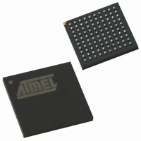
AT89C51SND2C-7FTUL Atmel, AT89C51SND2C-7FTUL Datasheet - Page 13

AT89C51SND2C-7FTUL
Manufacturer Part Number
AT89C51SND2C-7FTUL
Description
IC 8051 MCU FLASH 64K MP3 100BGA
Manufacturer
Atmel
Series
89Cr
Datasheet
1.AT89C51SND2C-7FTUL.pdf
(242 pages)
Specifications of AT89C51SND2C-7FTUL
Core Processor
8051
Core Size
8-Bit
Speed
40MHz
Connectivity
I²C, IDE/ATAPI, MMC, SPI, UART/USART, USB
Peripherals
Audio, I²S, MP3, PCM, POR, WDT
Number Of I /o
32
Program Memory Size
64KB (64K x 8)
Program Memory Type
FLASH
Ram Size
2.25K x 8
Voltage - Supply (vcc/vdd)
2.7 V ~ 3.3 V
Data Converters
A/D 2x10b; D/A 2x20b
Oscillator Type
Internal
Operating Temperature
-40°C ~ 85°C
Package / Case
100-TFBGA
Data Bus Width
8 bit
Data Ram Size
2.25 KB
Interface Type
ATAPI, I2S, IDE, SPI, UART, USB
Maximum Clock Frequency
40 MHz
Number Of Programmable I/os
32
Number Of Timers
2
Maximum Operating Temperature
+ 85 C
Mounting Style
SMD/SMT
Minimum Operating Temperature
- 40 C
Lead Free Status / RoHS Status
Lead free / RoHS Compliant
Eeprom Size
-
Lead Free Status / Rohs Status
Details
Other names
AT89C51SND2C7FTUL
Available stocks
Company
Part Number
Manufacturer
Quantity
Price
Company:
Part Number:
AT89C51SND2C-7FTUL
Manufacturer:
ATMEL
Quantity:
4 371
- Current page: 13 of 242
- Download datasheet (3Mb)
5. Clock Controller
5.1
4341H–MP3–10/07
Oscillator
The AT8xC51SND2C clock controller is based on an on-chip oscillator feeding an on-chip Phase
Lock Loop (PLL). All internal clocks to the peripherals and CPU core are generated by this
controller.
The AT8xC51SND2C X1 and X2 pins are the input and the output of a single-stage on-chip
inverter (see Figure 5-1) that can be configured with off-chip components such as a Pierce oscil-
lator (see Figure 5-2). Value of capacitors and crystal characteristics are detailed in the section
“DC Characteristics”.
The oscillator outputs three different clocks: a clock for the PLL, a clock for the CPU core, and a
clock for the peripherals as shown in Figure 5-1. These clocks are either enabled or disabled,
depending on the power reduction mode as detailed in the section
page
sampling clocks.
Figure 5-1.
Figure 5-2.
47. The peripheral clock is used to generate the Timer 0, Timer 1, MMC, SPI, and Port
X1
X2
Oscillator Block Diagram and Symbol
Crystal Connection
Peripheral Clock Symbol
CLOCK
PCON.1
PER
PD
VSS
CPU Core Clock Symbol
C1
C2
÷
2
CLOCK
CPU
AT8xC51SND2C/MP3B
CKCON.0
Q
X2
0
1
X1
X2
PCON.0
IDL
“Power Management” on
Oscillator Clock Symbol
CLOCK
OSC
Peripheral
Clock
CPU Core
Clock
Oscillator
Clock
13
Related parts for AT89C51SND2C-7FTUL
Image
Part Number
Description
Manufacturer
Datasheet
Request
R

Part Number:
Description:
DEV KIT FOR AVR/AVR32
Manufacturer:
Atmel
Datasheet:

Part Number:
Description:
INTERVAL AND WIPE/WASH WIPER CONTROL IC WITH DELAY
Manufacturer:
ATMEL Corporation
Datasheet:

Part Number:
Description:
Low-Voltage Voice-Switched IC for Hands-Free Operation
Manufacturer:
ATMEL Corporation
Datasheet:

Part Number:
Description:
MONOLITHIC INTEGRATED FEATUREPHONE CIRCUIT
Manufacturer:
ATMEL Corporation
Datasheet:

Part Number:
Description:
AM-FM Receiver IC U4255BM-M
Manufacturer:
ATMEL Corporation
Datasheet:

Part Number:
Description:
Monolithic Integrated Feature Phone Circuit
Manufacturer:
ATMEL Corporation
Datasheet:

Part Number:
Description:
Multistandard Video-IF and Quasi Parallel Sound Processing
Manufacturer:
ATMEL Corporation
Datasheet:

Part Number:
Description:
High-performance EE PLD
Manufacturer:
ATMEL Corporation
Datasheet:

Part Number:
Description:
8-bit Flash Microcontroller
Manufacturer:
ATMEL Corporation
Datasheet:

Part Number:
Description:
2-Wire Serial EEPROM
Manufacturer:
ATMEL Corporation
Datasheet:


