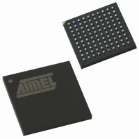
AT89C51SND2C-7FTUL Atmel, AT89C51SND2C-7FTUL Datasheet - Page 24

AT89C51SND2C-7FTUL
Manufacturer Part Number
AT89C51SND2C-7FTUL
Description
IC 8051 MCU FLASH 64K MP3 100BGA
Manufacturer
Atmel
Series
89Cr
Datasheet
1.AT89C51SND2C-7FTUL.pdf
(242 pages)
Specifications of AT89C51SND2C-7FTUL
Core Processor
8051
Core Size
8-Bit
Speed
40MHz
Connectivity
I²C, IDE/ATAPI, MMC, SPI, UART/USART, USB
Peripherals
Audio, I²S, MP3, PCM, POR, WDT
Number Of I /o
32
Program Memory Size
64KB (64K x 8)
Program Memory Type
FLASH
Ram Size
2.25K x 8
Voltage - Supply (vcc/vdd)
2.7 V ~ 3.3 V
Data Converters
A/D 2x10b; D/A 2x20b
Oscillator Type
Internal
Operating Temperature
-40°C ~ 85°C
Package / Case
100-TFBGA
Data Bus Width
8 bit
Data Ram Size
2.25 KB
Interface Type
ATAPI, I2S, IDE, SPI, UART, USB
Maximum Clock Frequency
40 MHz
Number Of Programmable I/os
32
Number Of Timers
2
Maximum Operating Temperature
+ 85 C
Mounting Style
SMD/SMT
Minimum Operating Temperature
- 40 C
Lead Free Status / RoHS Status
Lead free / RoHS Compliant
Eeprom Size
-
Lead Free Status / Rohs Status
Details
Other names
AT89C51SND2C7FTUL
Available stocks
Company
Part Number
Manufacturer
Quantity
Price
Company:
Part Number:
AT89C51SND2C-7FTUL
Manufacturer:
ATMEL
Quantity:
4 371
- Current page: 24 of 242
- Download datasheet (3Mb)
7. Data Memory
Figure 7-1.
7.1
7.1.1
24
Internal Space
AT8xC51SND2C/MP3B
Lower 128 Bytes RAM
7FFh
Internal and External Data Memory Organization
00h
Internal ERAM
EXTRAM = 0
2K Bytes
The AT8xC51SND2C provides data memory access in 2 different spaces:
1. The internal space mapped in three separate segments:
2. The external space.
A fourth internal segment is available but dedicated to Special Function Registers, SFRs,
(addresses 80h to FFh) accessible by direct addressing mode. For information on this segment,
refer to the Section “Special Function Registers”, page 31.
Figure 7-1 shows the internal and external data memory spaces organization.
The lower 128 Bytes of RAM (see Figure 7-2) are accessible from address 00h to 7Fh using
direct or indirect addressing modes. The lowest 32 Bytes are grouped into 4 banks of 8 registers
(R0 to R7). 2 bits RS0 and RS1 in PSW register (see Table 7-4) select which bank is in use
according to Table 7-1. This allows more efficient use of code space, since register instructions
are shorter than instructions that use direct addressing, and can be used for context switching in
interrupt service routines.
Table 7-1.
–
–
–
The lower 128 Bytes RAM segment
The upper 128 Bytes RAM segment
The expanded 2048 Bytes RAM segment
RS1
0
0
1
1
FFh
7Fh
80h
00h
Register Bank Selection
Indirect Addressing
Direct or Indirect
Internal RAM
Internal RAM
Addressing
128 Bytes
128 Bytes
Upper
Lower
RS0
0
1
0
1
FFh
80h
Direct Addressing
Description
Register bank 0 from 00h to 07h
Register bank 1 from 08h to 0Fh
Register bank 2 from 10h to 17h
Register bank 3 from 18h to 1Fh
Registers
Function
Special
FFFFh
0800h
0000h
External XRAM
EXTRAM = 1
64K Bytes
4341H–MP3–10/07
Related parts for AT89C51SND2C-7FTUL
Image
Part Number
Description
Manufacturer
Datasheet
Request
R

Part Number:
Description:
DEV KIT FOR AVR/AVR32
Manufacturer:
Atmel
Datasheet:

Part Number:
Description:
INTERVAL AND WIPE/WASH WIPER CONTROL IC WITH DELAY
Manufacturer:
ATMEL Corporation
Datasheet:

Part Number:
Description:
Low-Voltage Voice-Switched IC for Hands-Free Operation
Manufacturer:
ATMEL Corporation
Datasheet:

Part Number:
Description:
MONOLITHIC INTEGRATED FEATUREPHONE CIRCUIT
Manufacturer:
ATMEL Corporation
Datasheet:

Part Number:
Description:
AM-FM Receiver IC U4255BM-M
Manufacturer:
ATMEL Corporation
Datasheet:

Part Number:
Description:
Monolithic Integrated Feature Phone Circuit
Manufacturer:
ATMEL Corporation
Datasheet:

Part Number:
Description:
Multistandard Video-IF and Quasi Parallel Sound Processing
Manufacturer:
ATMEL Corporation
Datasheet:

Part Number:
Description:
High-performance EE PLD
Manufacturer:
ATMEL Corporation
Datasheet:

Part Number:
Description:
8-bit Flash Microcontroller
Manufacturer:
ATMEL Corporation
Datasheet:

Part Number:
Description:
2-Wire Serial EEPROM
Manufacturer:
ATMEL Corporation
Datasheet:


