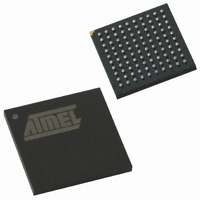
AT89C51SND2C-7FTUL Atmel, AT89C51SND2C-7FTUL Datasheet - Page 55

AT89C51SND2C-7FTUL
Manufacturer Part Number
AT89C51SND2C-7FTUL
Description
IC 8051 MCU FLASH 64K MP3 100BGA
Manufacturer
Atmel
Series
89Cr
Datasheet
1.AT89C51SND2C-7FTUL.pdf
(242 pages)
Specifications of AT89C51SND2C-7FTUL
Core Processor
8051
Core Size
8-Bit
Speed
40MHz
Connectivity
I²C, IDE/ATAPI, MMC, SPI, UART/USART, USB
Peripherals
Audio, I²S, MP3, PCM, POR, WDT
Number Of I /o
32
Program Memory Size
64KB (64K x 8)
Program Memory Type
FLASH
Ram Size
2.25K x 8
Voltage - Supply (vcc/vdd)
2.7 V ~ 3.3 V
Data Converters
A/D 2x10b; D/A 2x20b
Oscillator Type
Internal
Operating Temperature
-40°C ~ 85°C
Package / Case
100-TFBGA
Data Bus Width
8 bit
Data Ram Size
2.25 KB
Interface Type
ATAPI, I2S, IDE, SPI, UART, USB
Maximum Clock Frequency
40 MHz
Number Of Programmable I/os
32
Number Of Timers
2
Maximum Operating Temperature
+ 85 C
Mounting Style
SMD/SMT
Minimum Operating Temperature
- 40 C
Lead Free Status / RoHS Status
Lead free / RoHS Compliant
Eeprom Size
-
Lead Free Status / Rohs Status
Details
Other names
AT89C51SND2C7FTUL
Available stocks
Company
Part Number
Manufacturer
Quantity
Price
Company:
Part Number:
AT89C51SND2C-7FTUL
Manufacturer:
ATMEL
Quantity:
4 371
- Current page: 55 of 242
- Download datasheet (3Mb)
11.3.4
Figure 11-8. Timer/Counter 0 in Mode 3: 2 8-bit Counters
Figure 11-9. Mode 3 Overflow Period Formula
11.4
4341H–MP3–10/07
Timer 1
INT0
Mode 3 (2 8-bit Timers)
CLOCK
CLOCK
TIM0
TIM0
T0
GATE0
TMOD.3
÷ 6
÷ 6
Mode 3 configures Timer 0 such that registers TL0 and TH0 operate as separate 8-bit Timers
(see Figure 11-8). This mode is provided for applications requiring an additional 8-bit Timer or
Counter. TL0 uses the Timer 0 control bits C/T0# and GATE0 in TMOD register, and TR0 and
TF0 in TCON register in the normal manner. TH0 is locked into a Timer function (counting
F
ation of Timer 1 is restricted when Timer 0 is in mode 3. Figure 11-7 gives the autoreload period
calculation formulas for both TF0 and TF1 flags.
Timer 1 is identical to Timer 0 except for Mode 3 which is a hold-count mode. The following com-
ments help to understand the differences:
•
•
•
•
•
TF1
Timer 1 functions as either a Timer or event Counter in three modes of operation. Figure 11-
2 through Figure 11-6 show the logical configuration for modes 0, 1, and 2. Timer 1’s mode 3
is a hold-count mode.
Timer 1 is controlled by the four high-order bits of TMOD register (see Figure 11-2) and bits
2, 3, 6 and 7 of TCON register (see Figure 11-1). TMOD register selects the method of Timer
gating (GATE1), Timer or Counter operation (C/T1#) and mode of operation (M11 and M01).
TCON register provides Timer 1 control functions: overflow flag (TF1), run control bit (TR1),
interrupt flag (IE1) and interrupt type control bit (IT1).
Timer 1 can serve as the Baud Rate Generator for the Serial Port. Mode 2 is best suited for
this purpose.
For normal Timer operation (GATE1 = 0), setting TR1 allows TL1 to be incremented by the
selected input. Setting GATE1 and TR1 allows external pin INT1 to control Timer operation.
Timer 1 overflow (count rolls over from all 1s to all 0s) sets the TF1 flag generating an
interrupt request.
/6) and takes over use of the Timer 1 interrupt (TF1) and run control (TR1) bits. Thus, oper-
TMOD.2
C/T0#
TF0
0
1
PER
TCON.4
TR0
=
6
⋅
(256 – TL0)
TCON.6
F
TR1
TIM0
(8 bits)
(8 bits)
TH0
TL0
TF1
PER
=
AT8xC51SND2C/MP3B
6
Overflow
Overflow
⋅
(256 – TH0)
F
TIM0
TCON.5
TCON.7
TF0
TF1
Timer 0
Interrupt
Request
Timer 1
Interrupt
Request
55
Related parts for AT89C51SND2C-7FTUL
Image
Part Number
Description
Manufacturer
Datasheet
Request
R

Part Number:
Description:
DEV KIT FOR AVR/AVR32
Manufacturer:
Atmel
Datasheet:

Part Number:
Description:
INTERVAL AND WIPE/WASH WIPER CONTROL IC WITH DELAY
Manufacturer:
ATMEL Corporation
Datasheet:

Part Number:
Description:
Low-Voltage Voice-Switched IC for Hands-Free Operation
Manufacturer:
ATMEL Corporation
Datasheet:

Part Number:
Description:
MONOLITHIC INTEGRATED FEATUREPHONE CIRCUIT
Manufacturer:
ATMEL Corporation
Datasheet:

Part Number:
Description:
AM-FM Receiver IC U4255BM-M
Manufacturer:
ATMEL Corporation
Datasheet:

Part Number:
Description:
Monolithic Integrated Feature Phone Circuit
Manufacturer:
ATMEL Corporation
Datasheet:

Part Number:
Description:
Multistandard Video-IF and Quasi Parallel Sound Processing
Manufacturer:
ATMEL Corporation
Datasheet:

Part Number:
Description:
High-performance EE PLD
Manufacturer:
ATMEL Corporation
Datasheet:

Part Number:
Description:
8-bit Flash Microcontroller
Manufacturer:
ATMEL Corporation
Datasheet:

Part Number:
Description:
2-Wire Serial EEPROM
Manufacturer:
ATMEL Corporation
Datasheet:


