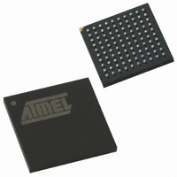
AT89C51SND2C-7FTUL Atmel, AT89C51SND2C-7FTUL Datasheet - Page 199

AT89C51SND2C-7FTUL
Manufacturer Part Number
AT89C51SND2C-7FTUL
Description
IC 8051 MCU FLASH 64K MP3 100BGA
Manufacturer
Atmel
Series
89Cr
Datasheet
1.AT89C51SND2C-7FTUL.pdf
(242 pages)
Specifications of AT89C51SND2C-7FTUL
Core Processor
8051
Core Size
8-Bit
Speed
40MHz
Connectivity
I²C, IDE/ATAPI, MMC, SPI, UART/USART, USB
Peripherals
Audio, I²S, MP3, PCM, POR, WDT
Number Of I /o
32
Program Memory Size
64KB (64K x 8)
Program Memory Type
FLASH
Ram Size
2.25K x 8
Voltage - Supply (vcc/vdd)
2.7 V ~ 3.3 V
Data Converters
A/D 2x10b; D/A 2x20b
Oscillator Type
Internal
Operating Temperature
-40°C ~ 85°C
Package / Case
100-TFBGA
Data Bus Width
8 bit
Data Ram Size
2.25 KB
Interface Type
ATAPI, I2S, IDE, SPI, UART, USB
Maximum Clock Frequency
40 MHz
Number Of Programmable I/os
32
Number Of Timers
2
Maximum Operating Temperature
+ 85 C
Mounting Style
SMD/SMT
Minimum Operating Temperature
- 40 C
Lead Free Status / RoHS Status
Lead free / RoHS Compliant
Eeprom Size
-
Lead Free Status / Rohs Status
Details
Other names
AT89C51SND2C7FTUL
Available stocks
Company
Part Number
Manufacturer
Quantity
Price
Company:
Part Number:
AT89C51SND2C-7FTUL
Manufacturer:
ATMEL
Quantity:
4 371
- Current page: 199 of 242
- Download datasheet (3Mb)
22. Analog to Digital Converter
22.1
4341H–MP3–10/07
Description
The AT8XSND2CMP3B implement a 2-channel 10-bit (8 true bits) analog to digital converter
(ADC). First channel of this ADC can be used for battery monitoring while the second one can
be used for voice sampling at 8 kHz.
The AT8xC51SND2C does not include the A/D converter.
The A/D converter interfaces with the C51 core through four special function registers: ADCON,
the ADC control register (see
and
As shown in Figure 22-1, the ADC is composed of a 10-bit cascaded potentiometric digital to
analog converter, connected to the negative input of a comparator. The output voltage of this
DAC is compared to the analog voltage stored in the Sample and Hold and coming from AIN0 or
AIN1 input depending on the channel selected (see Table 2). The 10-bit ADDAT converted
value (see formula in Figure 22-1) is delivered in ADDH and ADDL registers, ADDH is giving the
8 most significant bits while ADDL is giving the 2 least significant bits.
Figure 22-1. ADC Structure
Figure 22-2 shows the timing diagram of a complete conversion. For simplicity, the figure depicts
the waveforms in idealized form and do not provide precise timing information. For ADC charac-
teristics and timing parameters refer to the section “AC Characteristics”.
Table
AIN1
AIN0
6); and ADCLK, the ADC clock register (see Table 4).
CLOCK
ADC
ADDAT
ADCON.0
ADCS
0
1
=
1023 V
------------------------- -
Table
ADCON.5
Sample and Hold
V
ADEN
REF
⋅
CONTROL
IN
3); ADDH and ADDL, the ADC data registers (see
AVSS
ADCON.3
ADSST
+
-
AT8xC51SND2C/MP3B
AREFP
ADEOC
ADCON.4
R/2R DAC
AREFN
SAR
EADC
IEN1.3
8
2
10
ADDH
ADDL
ADC
Interrupt
Request
Table 5
199
Related parts for AT89C51SND2C-7FTUL
Image
Part Number
Description
Manufacturer
Datasheet
Request
R

Part Number:
Description:
DEV KIT FOR AVR/AVR32
Manufacturer:
Atmel
Datasheet:

Part Number:
Description:
INTERVAL AND WIPE/WASH WIPER CONTROL IC WITH DELAY
Manufacturer:
ATMEL Corporation
Datasheet:

Part Number:
Description:
Low-Voltage Voice-Switched IC for Hands-Free Operation
Manufacturer:
ATMEL Corporation
Datasheet:

Part Number:
Description:
MONOLITHIC INTEGRATED FEATUREPHONE CIRCUIT
Manufacturer:
ATMEL Corporation
Datasheet:

Part Number:
Description:
AM-FM Receiver IC U4255BM-M
Manufacturer:
ATMEL Corporation
Datasheet:

Part Number:
Description:
Monolithic Integrated Feature Phone Circuit
Manufacturer:
ATMEL Corporation
Datasheet:

Part Number:
Description:
Multistandard Video-IF and Quasi Parallel Sound Processing
Manufacturer:
ATMEL Corporation
Datasheet:

Part Number:
Description:
High-performance EE PLD
Manufacturer:
ATMEL Corporation
Datasheet:

Part Number:
Description:
8-bit Flash Microcontroller
Manufacturer:
ATMEL Corporation
Datasheet:

Part Number:
Description:
2-Wire Serial EEPROM
Manufacturer:
ATMEL Corporation
Datasheet:


