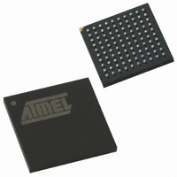
AT89C51SND2C-7FTUL Atmel, AT89C51SND2C-7FTUL Datasheet - Page 40

AT89C51SND2C-7FTUL
Manufacturer Part Number
AT89C51SND2C-7FTUL
Description
IC 8051 MCU FLASH 64K MP3 100BGA
Manufacturer
Atmel
Series
89Cr
Datasheet
1.AT89C51SND2C-7FTUL.pdf
(242 pages)
Specifications of AT89C51SND2C-7FTUL
Core Processor
8051
Core Size
8-Bit
Speed
40MHz
Connectivity
I²C, IDE/ATAPI, MMC, SPI, UART/USART, USB
Peripherals
Audio, I²S, MP3, PCM, POR, WDT
Number Of I /o
32
Program Memory Size
64KB (64K x 8)
Program Memory Type
FLASH
Ram Size
2.25K x 8
Voltage - Supply (vcc/vdd)
2.7 V ~ 3.3 V
Data Converters
A/D 2x10b; D/A 2x20b
Oscillator Type
Internal
Operating Temperature
-40°C ~ 85°C
Package / Case
100-TFBGA
Data Bus Width
8 bit
Data Ram Size
2.25 KB
Interface Type
ATAPI, I2S, IDE, SPI, UART, USB
Maximum Clock Frequency
40 MHz
Number Of Programmable I/os
32
Number Of Timers
2
Maximum Operating Temperature
+ 85 C
Mounting Style
SMD/SMT
Minimum Operating Temperature
- 40 C
Lead Free Status / RoHS Status
Lead free / RoHS Compliant
Eeprom Size
-
Lead Free Status / Rohs Status
Details
Other names
AT89C51SND2C7FTUL
Available stocks
Company
Part Number
Manufacturer
Quantity
Price
Company:
Part Number:
AT89C51SND2C-7FTUL
Manufacturer:
ATMEL
Quantity:
4 371
- Current page: 40 of 242
- Download datasheet (3Mb)
9.2
9.2.1
9.2.2
9.2.3
40
External Interrupts
AT8xC51SND2C/MP3B
INT1:0 Inputs
KIN0 Inputs
Input Sampling
External interrupts INT0 and INT1 (INTn, n = 0 or 1) pins may each be programmed to be level-
triggered or edge-triggered, dependent upon bits IT0 and IT1 (ITn, n = 0 or 1) in TCON register
as shown in Figure 9-2. If ITn = 0, INTn is triggered by a low level at the pin. If ITn = 1, INTn is
negative-edge triggered. External interrupts are enabled with bits EX0 and EX1 (EXn, n = 0 or 1)
in IEN0. Events on INTn set the interrupt request flag IEn in TCON register. If the interrupt is
edge-triggered, the request flag is cleared by hardware when vectoring to the interrupt service
routine. If the interrupt is level-triggered, the interrupt service routine must clear the request flag
and the interrupt must be deasserted before the end of the interrupt service routine.
INT0 and INT1 inputs provide both the capability to exit from Power-down mode on low level sig-
nals as detailed in section “Exiting Power-down Mode”, page 50.
Figure 9-2.
External interrupts KIN0 provides the capability to connect a keyboard. For detailed information
on this inputs, refer to section “Keyboard Interface”, page 204.
External interrupt pins (INT1:0 and KIN0) are sampled once per peripheral cycle (6 peripheral
clock periods) (see Figure 9-3). A level-triggered interrupt pin held low or high for more than 6
peripheral clock periods (12 oscillator in standard mode or 6 oscillator clock periods in X2 mode)
guarantees detection. Edge-triggered external interrupts must hold the request pin low for at
least 6 peripheral clock periods.
Figure 9-3.
INT0/1
INT1:0 Input Circuitry
Minimum Pulse Timings
Level-Triggered Interrupt
Edge-Triggered Interrupt
TCON.0/2
IT0/1
0
1
1 cycle
> 1 Peripheral Cycle
> 1 Peripheral Cycle
TCON.1/3
IE0/1
1 cycle
1 cycle
IEN0.0/2
EX0/1
INT0/1
Interrupt
Request
4341H–MP3–10/07
Related parts for AT89C51SND2C-7FTUL
Image
Part Number
Description
Manufacturer
Datasheet
Request
R

Part Number:
Description:
DEV KIT FOR AVR/AVR32
Manufacturer:
Atmel
Datasheet:

Part Number:
Description:
INTERVAL AND WIPE/WASH WIPER CONTROL IC WITH DELAY
Manufacturer:
ATMEL Corporation
Datasheet:

Part Number:
Description:
Low-Voltage Voice-Switched IC for Hands-Free Operation
Manufacturer:
ATMEL Corporation
Datasheet:

Part Number:
Description:
MONOLITHIC INTEGRATED FEATUREPHONE CIRCUIT
Manufacturer:
ATMEL Corporation
Datasheet:

Part Number:
Description:
AM-FM Receiver IC U4255BM-M
Manufacturer:
ATMEL Corporation
Datasheet:

Part Number:
Description:
Monolithic Integrated Feature Phone Circuit
Manufacturer:
ATMEL Corporation
Datasheet:

Part Number:
Description:
Multistandard Video-IF and Quasi Parallel Sound Processing
Manufacturer:
ATMEL Corporation
Datasheet:

Part Number:
Description:
High-performance EE PLD
Manufacturer:
ATMEL Corporation
Datasheet:

Part Number:
Description:
8-bit Flash Microcontroller
Manufacturer:
ATMEL Corporation
Datasheet:

Part Number:
Description:
2-Wire Serial EEPROM
Manufacturer:
ATMEL Corporation
Datasheet:


