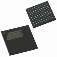
AT89C51SND2C-7FTUL Atmel, AT89C51SND2C-7FTUL Datasheet - Page 16

AT89C51SND2C-7FTUL
Manufacturer Part Number
AT89C51SND2C-7FTUL
Description
IC 8051 MCU FLASH 64K MP3 100BGA
Manufacturer
Atmel
Series
89Cr
Datasheet
1.AT89C51SND2C-7FTUL.pdf
(242 pages)
Specifications of AT89C51SND2C-7FTUL
Core Processor
8051
Core Size
8-Bit
Speed
40MHz
Connectivity
I²C, IDE/ATAPI, MMC, SPI, UART/USART, USB
Peripherals
Audio, I²S, MP3, PCM, POR, WDT
Number Of I /o
32
Program Memory Size
64KB (64K x 8)
Program Memory Type
FLASH
Ram Size
2.25K x 8
Voltage - Supply (vcc/vdd)
2.7 V ~ 3.3 V
Data Converters
A/D 2x10b; D/A 2x20b
Oscillator Type
Internal
Operating Temperature
-40°C ~ 85°C
Package / Case
100-TFBGA
Data Bus Width
8 bit
Data Ram Size
2.25 KB
Interface Type
ATAPI, I2S, IDE, SPI, UART, USB
Maximum Clock Frequency
40 MHz
Number Of Programmable I/os
32
Number Of Timers
2
Maximum Operating Temperature
+ 85 C
Mounting Style
SMD/SMT
Minimum Operating Temperature
- 40 C
Lead Free Status / RoHS Status
Lead free / RoHS Compliant
Eeprom Size
-
Lead Free Status / Rohs Status
Details
Other names
AT89C51SND2C7FTUL
Available stocks
Company
Part Number
Manufacturer
Quantity
Price
Company:
Part Number:
AT89C51SND2C-7FTUL
Manufacturer:
ATMEL
Quantity:
4 371
- Current page: 16 of 242
- Download datasheet (3Mb)
5.4
16
Registers
AT8xC51SND2C/MP3B
Table 5-1.
Reset Value = 0000 000Xb (AT89C51SND2C) or 0000 0000b (AT83SND2C)
Table 5-2.
Bit Number
Bit Number
TWIX2
7 - 6
5 - 4
R1
7
7
6
5
4
3
2
1
0
7
3
2
Mnemonic
Mnemonic
PLLRES
CKCON Register
CKCON (S:8Fh) – Clock Control Register
PLLCON Register
PLLCON (S:E9h) – PLL Control Register
TWIX2
WDX2
WDX2
T1X2
T0X2
SIX2
R1:0
Bit
Bit
X2
R0
6
6
-
-
-
-
Description
Two-Wire Clock Control Bit
Set to select the oscillator clock divided by 2 as TWI clock input (X2 independent).
Clear to select the peripheral clock as TWI clock input (X2 dependent).
Watchdog Clock Control Bit
Set to select the oscillator clock divided by 2 as watchdog clock input (X2 independent).
Clear to select the peripheral clock as watchdog clock input (X2 dependent).
Reserved
The values read from this bit is indeterminate. Do not set this bit.
Enhanced UART Clock (Mode 0 and 2) Control Bit
Set to select the oscillator clock divided by 2 as UART clock input (X2 independent).
Clear to select the peripheral clock as UART clock input (X2 dependent)..
Reserved
The values read from this bit is indeterminate. Do not set this bit.
Timer 1 Clock Control Bit
Set to select the oscillator clock divided by 2 as timer 1 clock input (X2 independent).
Clear to select the peripheral clock as timer 1 clock input (X2 dependent).
Timer 0 Clock Control Bit
Set to select the oscillator clock divided by 2 as timer 0 clock input (X2 independent).
Clear to select the peripheral clock as timer 0 clock input (X2 dependent).
System Clock Control Bit
Clear to select 12 clock periods per machine cycle (STD mode, F
Set to select 6 clock periods per machine cycle (X2 mode, F
Description
PLL Least Significant Bits R Divider
2 LSB of the 10-bit R divider.
Reserved
The values read from these bits are always 0. Do not set these bits.
PLL Reset Bit
Set this bit to reset the PLL.
Clear this bit to free the PLL and allow enabling.
Reserved
The value read from this bit is always 0. Do not set this bit.
5
5
-
-
SIX2
4
4
-
PLLRES
3
3
-
T1X2
2
2
-
CPU
PLLEN
T0X2
= F
CPU
1
1
PER
= F
4341H–MP3–10/07
= F
PER
OSC
PLOCK
= F
).
X2
0
0
OSC
/
2).
Related parts for AT89C51SND2C-7FTUL
Image
Part Number
Description
Manufacturer
Datasheet
Request
R

Part Number:
Description:
DEV KIT FOR AVR/AVR32
Manufacturer:
Atmel
Datasheet:

Part Number:
Description:
INTERVAL AND WIPE/WASH WIPER CONTROL IC WITH DELAY
Manufacturer:
ATMEL Corporation
Datasheet:

Part Number:
Description:
Low-Voltage Voice-Switched IC for Hands-Free Operation
Manufacturer:
ATMEL Corporation
Datasheet:

Part Number:
Description:
MONOLITHIC INTEGRATED FEATUREPHONE CIRCUIT
Manufacturer:
ATMEL Corporation
Datasheet:

Part Number:
Description:
AM-FM Receiver IC U4255BM-M
Manufacturer:
ATMEL Corporation
Datasheet:

Part Number:
Description:
Monolithic Integrated Feature Phone Circuit
Manufacturer:
ATMEL Corporation
Datasheet:

Part Number:
Description:
Multistandard Video-IF and Quasi Parallel Sound Processing
Manufacturer:
ATMEL Corporation
Datasheet:

Part Number:
Description:
High-performance EE PLD
Manufacturer:
ATMEL Corporation
Datasheet:

Part Number:
Description:
8-bit Flash Microcontroller
Manufacturer:
ATMEL Corporation
Datasheet:

Part Number:
Description:
2-Wire Serial EEPROM
Manufacturer:
ATMEL Corporation
Datasheet:


