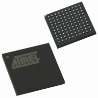
AT89C51SND2C-7FTUL Atmel, AT89C51SND2C-7FTUL Datasheet - Page 85

AT89C51SND2C-7FTUL
Manufacturer Part Number
AT89C51SND2C-7FTUL
Description
IC 8051 MCU FLASH 64K MP3 100BGA
Manufacturer
Atmel
Series
89Cr
Datasheet
1.AT89C51SND2C-7FTUL.pdf
(242 pages)
Specifications of AT89C51SND2C-7FTUL
Core Processor
8051
Core Size
8-Bit
Speed
40MHz
Connectivity
I²C, IDE/ATAPI, MMC, SPI, UART/USART, USB
Peripherals
Audio, I²S, MP3, PCM, POR, WDT
Number Of I /o
32
Program Memory Size
64KB (64K x 8)
Program Memory Type
FLASH
Ram Size
2.25K x 8
Voltage - Supply (vcc/vdd)
2.7 V ~ 3.3 V
Data Converters
A/D 2x10b; D/A 2x20b
Oscillator Type
Internal
Operating Temperature
-40°C ~ 85°C
Package / Case
100-TFBGA
Data Bus Width
8 bit
Data Ram Size
2.25 KB
Interface Type
ATAPI, I2S, IDE, SPI, UART, USB
Maximum Clock Frequency
40 MHz
Number Of Programmable I/os
32
Number Of Timers
2
Maximum Operating Temperature
+ 85 C
Mounting Style
SMD/SMT
Minimum Operating Temperature
- 40 C
Lead Free Status / RoHS Status
Lead free / RoHS Compliant
Eeprom Size
-
Lead Free Status / Rohs Status
Details
Other names
AT89C51SND2C7FTUL
Available stocks
Company
Part Number
Manufacturer
Quantity
Price
Company:
Part Number:
AT89C51SND2C-7FTUL
Manufacturer:
ATMEL
Quantity:
4 371
- Current page: 85 of 242
- Download datasheet (3Mb)
15.1.4
Figure 15-8. DAC SPI Interface Timings
4341H–MP3–10/07
DAC Interface SPI Protocol
AUDCDOUT
AUDCCLK
AUDCCS
AUDCDIN
Figure 15-7. Dac SPI Interface
On AUDCDIN, the first bit is a read/write bit. 0 indicates a write operation while 1 is for a read
operation. The 7 following bits are used for the register address and the 8 last ones are the write
data. For both address and data, the most significant bit is the first one.
In case of a read operation, AUDCDOUT provides the contents of the read register, MSB first.
The transfer is enabled by the AUDCCS signal active low. The interface is resetted at every ris-
ing edge of AUDCCS in order to come back to an idle state, even if the transfer does not
succeed. The DAC Interface SPI is synchronized with the serial clock AUDCCLK. Falling edge
latches AUDCDIN input and rising edge shifts AUDCDOUT output bits.
Note that the DLCK must run during any DAC SPI interface access (read or write).
AUDCCS
AUDCCLK
AUDCDIN
AUDCDOUT
Tssen
Tdsdo
rw a6 a5 a4 a3 a2 a1
Tssdi
Thsdi
Twl
a0
AT8xC51SND2C/MP3B
Tc
d7
d7 d6 d5 d4
Thsdo
d6
Twh
d5
d4
d3
d3
d2
d2
d1
d1 d0
Thsen
d0
85
Related parts for AT89C51SND2C-7FTUL
Image
Part Number
Description
Manufacturer
Datasheet
Request
R

Part Number:
Description:
DEV KIT FOR AVR/AVR32
Manufacturer:
Atmel
Datasheet:

Part Number:
Description:
INTERVAL AND WIPE/WASH WIPER CONTROL IC WITH DELAY
Manufacturer:
ATMEL Corporation
Datasheet:

Part Number:
Description:
Low-Voltage Voice-Switched IC for Hands-Free Operation
Manufacturer:
ATMEL Corporation
Datasheet:

Part Number:
Description:
MONOLITHIC INTEGRATED FEATUREPHONE CIRCUIT
Manufacturer:
ATMEL Corporation
Datasheet:

Part Number:
Description:
AM-FM Receiver IC U4255BM-M
Manufacturer:
ATMEL Corporation
Datasheet:

Part Number:
Description:
Monolithic Integrated Feature Phone Circuit
Manufacturer:
ATMEL Corporation
Datasheet:

Part Number:
Description:
Multistandard Video-IF and Quasi Parallel Sound Processing
Manufacturer:
ATMEL Corporation
Datasheet:

Part Number:
Description:
High-performance EE PLD
Manufacturer:
ATMEL Corporation
Datasheet:

Part Number:
Description:
8-bit Flash Microcontroller
Manufacturer:
ATMEL Corporation
Datasheet:

Part Number:
Description:
2-Wire Serial EEPROM
Manufacturer:
ATMEL Corporation
Datasheet:


