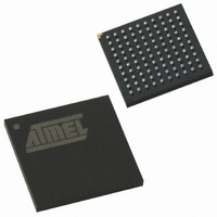
AT89C51SND2C-7FTUL Atmel, AT89C51SND2C-7FTUL Datasheet - Page 172

AT89C51SND2C-7FTUL
Manufacturer Part Number
AT89C51SND2C-7FTUL
Description
IC 8051 MCU FLASH 64K MP3 100BGA
Manufacturer
Atmel
Series
89Cr
Datasheet
1.AT89C51SND2C-7FTUL.pdf
(242 pages)
Specifications of AT89C51SND2C-7FTUL
Core Processor
8051
Core Size
8-Bit
Speed
40MHz
Connectivity
I²C, IDE/ATAPI, MMC, SPI, UART/USART, USB
Peripherals
Audio, I²S, MP3, PCM, POR, WDT
Number Of I /o
32
Program Memory Size
64KB (64K x 8)
Program Memory Type
FLASH
Ram Size
2.25K x 8
Voltage - Supply (vcc/vdd)
2.7 V ~ 3.3 V
Data Converters
A/D 2x10b; D/A 2x20b
Oscillator Type
Internal
Operating Temperature
-40°C ~ 85°C
Package / Case
100-TFBGA
Data Bus Width
8 bit
Data Ram Size
2.25 KB
Interface Type
ATAPI, I2S, IDE, SPI, UART, USB
Maximum Clock Frequency
40 MHz
Number Of Programmable I/os
32
Number Of Timers
2
Maximum Operating Temperature
+ 85 C
Mounting Style
SMD/SMT
Minimum Operating Temperature
- 40 C
Lead Free Status / RoHS Status
Lead free / RoHS Compliant
Eeprom Size
-
Lead Free Status / Rohs Status
Details
Other names
AT89C51SND2C7FTUL
Available stocks
Company
Part Number
Manufacturer
Quantity
Price
Company:
Part Number:
AT89C51SND2C-7FTUL
Manufacturer:
ATMEL
Quantity:
4 371
- Current page: 172 of 242
- Download datasheet (3Mb)
20.4.0.2
20.4.1
20.4.2
20.4.3
172
AT8xC51SND2C/MP3B
Transmission (Modes 1, 2 and 3)
Reception (Modes 1, 2 and 3)
Framing Error Detection (Modes 1, 2 and 3)
Modes 2 and 3
Figure 20-9. Data Frame Format (Mode 1)
Modes 2 and 3 are full-duplex, asynchronous modes. The data frame (see Figure 20-10) con-
sists of 11 bits: one start bit, eight data bits (transmitted and received LSB first), one
programmable ninth data bit and one stop bit. Serial data is transmitted on the TXD pin and
received on the RXD pin. On receive, the ninth bit is read from RB8 bit in SCON register. On
transmit, the ninth data bit is written to TB8 bit in SCON register. Alternatively, you can use the
ninth bit can be used as a command/data flag.
Figure 20-10. Data Frame Format (Modes 2 and 3)
To initiate a transmission, write to SCON register, set the SM0 and SM1 bits according to
Table 20-1, and set the ninth bit by writing to TB8 bit. Then, writing the Byte to be transmitted to
SBUF register starts the transmission.
To prepare for reception, write to SCON register, set the SM0 and SM1 bits according to
Table 20-1, and set the REN bit. The actual reception is then initiated by a detected high-to-low
transition on the RXD pin.
Framing error detection is provided for the three asynchronous modes. To enable the framing bit
error detection feature, set SMOD0 bit in PCON register as shown in Figure 20-11.
When this feature is enabled, the receiver checks each incoming data frame for a valid stop bit.
An invalid stop bit may result from noise on the serial lines or from simultaneous transmission by
2 devices. If a valid stop bit is not found, the software sets FE bit in SCON register.
Software may examine FE bit after each reception to check for data errors. Once set, only soft-
ware or a chip reset clear FE bit. Subsequently received frames with valid stop bits cannot clear
FE bit. When the framing error detection feature is enabled, RI rises on stop bit instead of the
last data bit as detailed in Figure 20-17.
Figure 20-11. Framing Error Block Diagram
Mode 1
Start bit
Start bit
Framing Error
D0
Controller
D0
D1
D1
D2
FE
D2
SM0
D3
9-bit data
D3
SMOD0
8-bit data
PCON.6
D4
1
0
D4
D5
D5
D6
SM0/FE
SCON.7
D6
D7
D7
D8
Stop bit
4341H–MP3–10/07
Stop bit
Related parts for AT89C51SND2C-7FTUL
Image
Part Number
Description
Manufacturer
Datasheet
Request
R

Part Number:
Description:
DEV KIT FOR AVR/AVR32
Manufacturer:
Atmel
Datasheet:

Part Number:
Description:
INTERVAL AND WIPE/WASH WIPER CONTROL IC WITH DELAY
Manufacturer:
ATMEL Corporation
Datasheet:

Part Number:
Description:
Low-Voltage Voice-Switched IC for Hands-Free Operation
Manufacturer:
ATMEL Corporation
Datasheet:

Part Number:
Description:
MONOLITHIC INTEGRATED FEATUREPHONE CIRCUIT
Manufacturer:
ATMEL Corporation
Datasheet:

Part Number:
Description:
AM-FM Receiver IC U4255BM-M
Manufacturer:
ATMEL Corporation
Datasheet:

Part Number:
Description:
Monolithic Integrated Feature Phone Circuit
Manufacturer:
ATMEL Corporation
Datasheet:

Part Number:
Description:
Multistandard Video-IF and Quasi Parallel Sound Processing
Manufacturer:
ATMEL Corporation
Datasheet:

Part Number:
Description:
High-performance EE PLD
Manufacturer:
ATMEL Corporation
Datasheet:

Part Number:
Description:
8-bit Flash Microcontroller
Manufacturer:
ATMEL Corporation
Datasheet:

Part Number:
Description:
2-Wire Serial EEPROM
Manufacturer:
ATMEL Corporation
Datasheet:


